| Search for content and authors |
ZnO and core/shell ZnO/ZnS nanofibers: Characterization and applications |
| Anna Baranowska-Korczyc , Krzysztof Fronc , Bożena Sikora , Izabela Kamińska , Kamil Sobczak , Anna Reszka , Krzysztof Dybko , Łukasz Kłopotowski , Wojciech Paszkowicz , Piotr Dłużewski , Bogdan J. Kowalski , Danek Elbaum |
|
Polish Academy of Sciences, Institute of Physics, al. Lotników 32/46, Warszawa 02-668, Poland |
| Abstract |
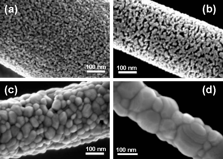
One-dimensional zinc oxide (ZnO) nanostructures are of interest because of their potential applications in electronics and optoelectronics. We synthesized ceramic ZnO nanofibers. The first step was to form the nanofibres by electrospinning technique using a suspension of zinc acetate in poly(vinyl alcohol) (PVA) as precursor. These composite one–dimensional nanostructures were calcined in air (400°C - 900°C) in order to remove organic components and obtain ZnO nanofibers [1]. Then, we synthesized ZnS shell on the ZnO nanofiber by the hydrogen sulphide treatment. Structural and chemical characterization was performed by X-ray diffraction (XRD), Transmission Electron Microscopy (TEM), Electron Energy Loss Spectroscopy (EELS), Scanning Electron Microscopy (SEM), Energy Dispersive X-ray Spectroscopy (EDX) and Atomic Force Microscopy (AFM). Additionally, optical characterization was done by a photoluminescence (PL) and cathodoluminescence measurements. The studies revealed nanofibers diameters ranging from 100 to 300 nm. Moreover, the nanofibers consisted of ZnO wurtzite crystals. The activation energy for the crystal-growth was estimated to be 12 kJ/mol. The average crystal diameter was 6.3 nm for nanofibers calcined at 500°C. Increased ZnO crystal sizes (Fig. 1) and intensity of the band gap emission were observed for higher calcination temperatures. The ZnS shell consisted of about 2 nm cubic crystals. We find that the light is emitted uniformly from all the fibers. Both CL and PL spectra, consist of two emission bands. One, centered around 380 nm, is related to the interband recombination. The other one centered around 550 nm is a defect band, and most probably originates from oxygen vacancies. The nanofibers can be applied to construct sensors and bio-sensors [2]. The Field Effect Transistors (FETs) based on semiconducting electrospun nanofibers are very promising real-time detectors. The nanofibers for FETs were calcined at 500º C for 4 h. We observed the current increase when the nanofibers were immersed in liquids (water and ethanol). Moreover, the current increased by three orders of magnitude when the nanofibers were exposed to the light (325 nm). For fabrication of biosensors based on the ZnO nanofibers, a surface passivation is required. In order to do that we synthesized core/shell ZnO/ZnS nanofibers and prepared a FET based on these fibers for biosensing applications.
Fig. 1. SEM images of ZnO nanofibers calcined at 400 (a), 500 (b), 650 (c) and 800°C for 4h. The research was supported by the European Union within European Regional Development Fund, through grant Innovative Economy (POIG.01.01.02-00-008/08), and by the Ministry of Science and Higher Education (Poland) through Grant No. N518 424036. 1. J.Y. Park, S.S. Kim., Growth of Nanograins in Electrospun ZnO Nanofibers, J Am. Ceram. Soc. 92 [8] 1691–1694 (2009). 2. V. Pachauri, A. Vlandas, K. Kern, K. Balasubramanian, Site-specific self-assembled liquid-gated ZnO nanowire transistors for sensing applications, Small, 6 [4], 589-594 (2010). |
| Legal notice |
|
| Related papers |
Presentation: Poster at IX Krajowe Sympozjum Użytkowników Promieniowania Synchrotronowego, by Anna Baranowska-KorczycSee On-line Journal of IX Krajowe Sympozjum Użytkowników Promieniowania Synchrotronowego Submitted: 2011-06-02 15:59 Revised: 2011-06-21 16:10 |