| Search for content and authors |
Dual-acceptor doped p-ZnO:(As+Sb)/n-GaN heterojunctions grown by PA-MBE as a highly selective UV detector |
| Ewa Przezdziecka , Krzysztof Gościński , Aleksandra Wierzbicka , Marcin Stachowicz , Anna Reszka , Anna Droba , Rafał Jakieła , Jacek M. Sajkowski , Mieczyslaw A. Pietrzyk , A Kozanecki |
|
Polish Academy of Sciences, Institute of Physics, al. Lotników 32/46, Warszawa 02-668, Poland |
| Abstract |
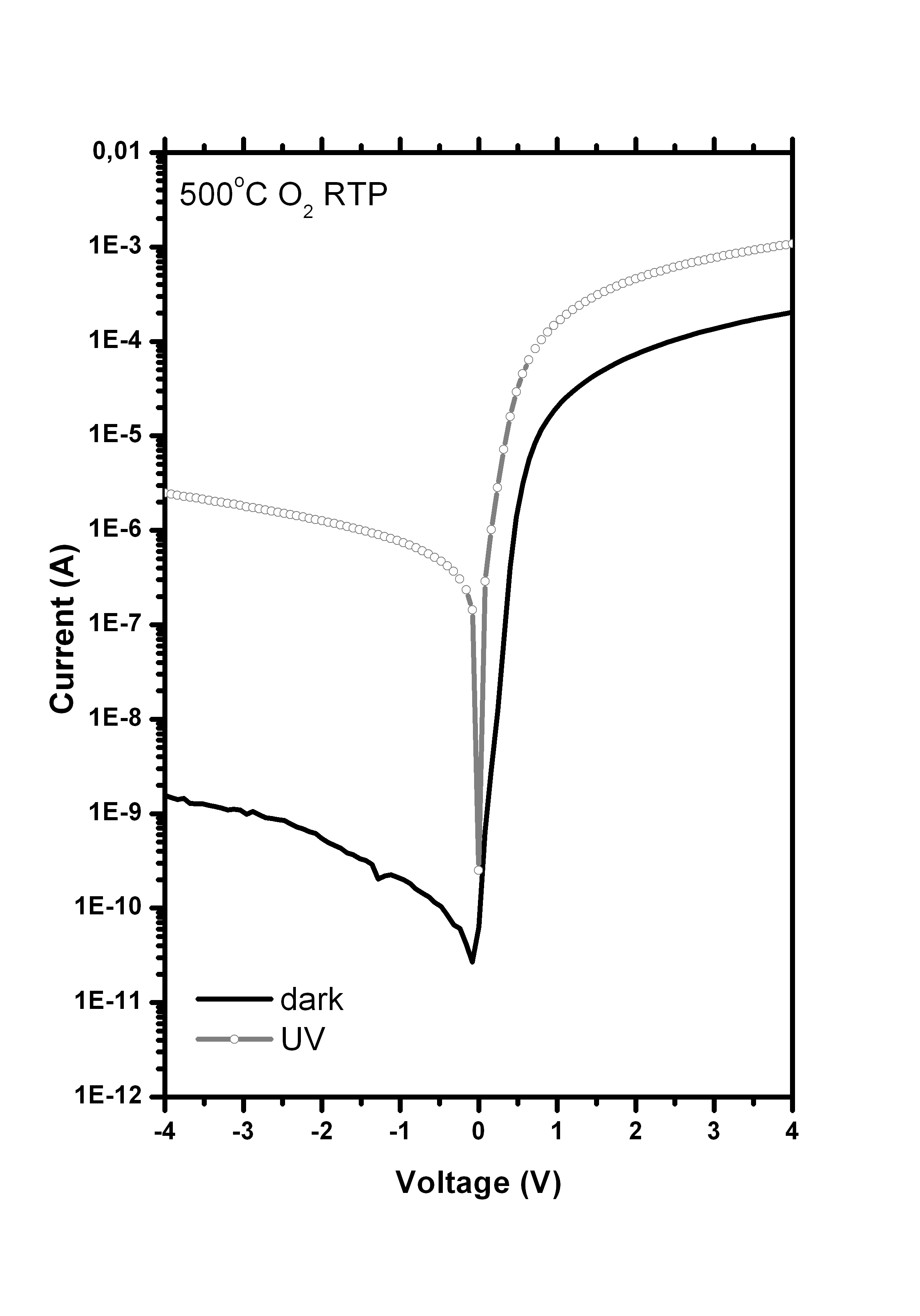
Zinc oxide (ZnO) is a promising candidate for application in ultraviolet (UV) photodetectors due to the large direct band gap and the high absorption coefficient in the UV spectrum range. UV detectors based on wide bandgap semiconductors like SiC, GaN and ZnO have received more and more attention due to their chemical and thermal stability in harsh environments. For applications in p-n diode detectors p-type doping of ZnO is necessary. It is known, however, that it is a difficult task due to the background n-type doping . High quality dual acceptor doped ZnO:(As,Sb) films were grown on n-type GaN templates by plasma-assisted Molecular Beam Epitaxy (PA-MBE)and p-ZnO/n-GaN heterojunction structures have been fabricated [1]. The structure consists of a 3.5 um thick GaN layer on sapphire substrate covered by a 60 nm thick As and Sb-doped ZnO film. The quality of the heterojunction was examined by X-ray diffraction, atomic force microscopy (AFM) and scanning electron microscopy (SEM). The As and Sb concentration in ZnO, measured by secondary ion mass spectroscopy (SIMS), is 1x1020 cm-3. The maximum forward-to-reverse current ratio IF/IR in the obtained diode is of about 105 at the applied voltage of ±4 V, which is a very good result for this type of heterojunction. Electronic properties were examined by XPS study and the presence of As acceptors was also confirmed by low temperature PL study. Photodetector’s response to the pulse of light in the UV region is relatively fast <<1 ms. Photodetectors based on a presented diodes are highly selective (FWHM photocurrent peak ~12 nm), work both in atmospheric pressure and in vacuum. 
Fig 1 Cuurent-voltage characteristics ZnO/GaN diodes dark and with UV illumination. The research was partially supported by the European Union within European Regional Development Fund, through grant Innovative Economy (POIG.01.01.02-00-008/08).
[1]E. Przeździecka, K. Gościński, M. Stachowicz, D. Dobosz, E. Zielony, J. M. Sajkowski, M. A. Pietrzyk, E. Płaczek-Popko, A. Kozanecki Sensors & Actuators: A. Physical (2013), pp. 27-31 |
| Legal notice |
|
| Related papers |
Presentation: Poster at 17th International Conference on Crystal Growth and Epitaxy - ICCGE-17, Topical Session 3, by Ewa PrzezdzieckaSee On-line Journal of 17th International Conference on Crystal Growth and Epitaxy - ICCGE-17 Submitted: 2013-03-26 14:15 Revised: 2013-07-18 12:05 |