| Search for content and authors |
Measurements of strain in AlGaN/GaN HEMT structures grown by plasma assisted molecular beam epitaxy |
| Jolanta Borysiuk 1, Kamil Sobczak 1, Aleksandra Wierzbicka 1, Kamil Klosek 1, Marta Sobanska 1, Zbigniew R. Zytkiewicz 1, Boleslaw L. Lucznik 2 |
|
1. Institute of Physics, Polish Academy of Sciences, Warsaw 02-668, Poland |
| Abstract |
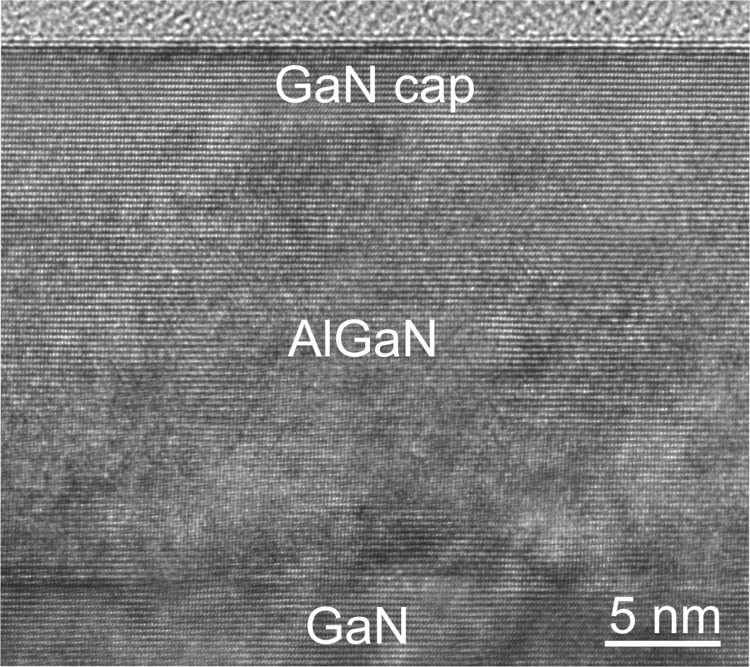
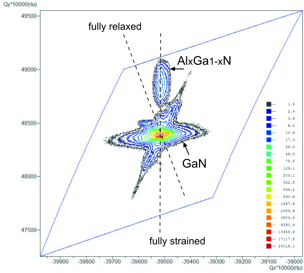
The AlGaN/GaN high electron mobility transistor (HEMT) structures were grown on the (0001) HVPE bulk GaN substrates using plasma-assisted molecular-beam epitaxy (PAMBE). The AlGaN layers of content of 12% or 20% were grown to nominal 20nm thickness and the 3nm thick GaN cap was added. High-resolution X-ray diffraction (HRXRD) measurements were used to determine crystallographic quality of HEMT structures. Built-in strain was obtained from peak intensity analysis. An effective lattice constant was derived from the shifts of the peaks positions. These X-ray data were compared to local measurements performed by transmission electron microscopy (TEM) – Fig.1. Tetragonal distortion was used for lattice strain in the interface regions. Structure geometry was also obtained from TEM images. Overall quality of the structures and their performance was assessed. Figure 1. TEM image of HEMT structure. Figure 1. TEM image of HEMT structure. 
Figure 2. XRD map of the (11 4) reflection. Acknowledgements This work was partially supported by the European Union within European Regional Development Found, through grant Innovative Economy POIG.01.01.02-00-008/08 NanoBiom. One of the authors (JB) wishes to thank the National Science Centre (Poland) support by grant DEC-2011/03/B/ST5/02698. |
| Legal notice |
|
| Related papers |
Presentation: Poster at 17th International Conference on Crystal Growth and Epitaxy - ICCGE-17, General Session 5, by Jolanta BorysiukSee On-line Journal of 17th International Conference on Crystal Growth and Epitaxy - ICCGE-17 Submitted: 2013-04-15 19:04 Revised: 2013-07-26 09:03 |