| Search for content and authors |
Optimization of nitrogen plasma source parameters for growth of GaN by MBE |
| Kamil Klosek , Marta Sobanska , Giorgi Tchutchulashvili , H. Teisseyre , Lukasz Klopotowski , Zbigniew R. Zytkiewicz |
|
Institute of Physics, Polish Academy of Sciences, Warsaw 02-668, Poland |
| Abstract |
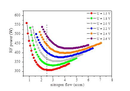
| It is already well known that the best GaN layers obtained by plasma-assisted molecular beam epitaxy (PAMBE) are grown under Ga-rich conditions with a bilayer of gallium present on the surface. Since under such conditions the growth is limited by flux of active nitrogen fine tuning of nitrogen source must be used for precise growth. An optical Si sensor was used to measure the light intensity emitted by the nitrogen source in the wavelength range of 750 to 850 nm. The sensor converts light emitted by the plasma into output voltage U. Nitrogen plasma intensity, and so the optical sensor output voltage U, depends both on the RF power and the nitrogen gas flow. This is illustrated in Fig. 1 that shows broad range of RF power and nitrogen flow parameters giving fixed value of sensor output U. 
Fig. 1: Set of RF power and nitrogen flow parameters for a fixed value of sensor output voltage U. In Fig. 2 the GaN growth rate vs. nitrogen flow is plotted for U = 1.5 V and U = 2.4 V. For each point the gallium flux was adjusted to keep the surface covered by 2 ML of Ga. As seen, the growth rate does not change when the plasma parameters vary along the red (U = 1.5 V) and the orange (U = 2.4 V) curves in Fig. 1. On the contrary, the growth rate monotonically increases with intensity of light emitted by nitrogen plasma as shown in Fig. 3. Since under gallium-rich conditions growth is controlled by nitrogen flux, results shown in Figs. 2-3 clearly indicate that the optical sensor output signal is a direct measure of the amount of active nitrogen species available for growth. Optical spectra of the plasma were measured to check how intensity of light emitted by atomic and molecular nitrogen species depend on nitrogen flow and RF power of the cell.
Fig. 2: GaN growth rate vs. nitrogen flow for U=1.5 V and U=2.4 V.
A procedure is presented allowing to find an optimal conditions of the plasma cell for high-quality GaN growth. Under these conditions the nitrogen flux contains maximum amount of excited metastable molecules and minimal amount of ionic and atomic nitrogen species to minimize GaN lattice damage, even at high growth rates. This work was supported by the European Union within European Regional Development Fund, through grant Innovative Economy (POIG.01.01.02-00-008/08 NanoBiom). |
| Legal notice |
|
| Related papers |
Presentation: Poster at 15th Summer School on Crystal Growth - ISSCG-15, by Kamil KlosekSee On-line Journal of 15th Summer School on Crystal Growth - ISSCG-15 Submitted: 2013-07-02 13:40 Revised: 2013-07-02 14:03 |