| Search for content and authors |
Optical properties of GaAs:Mn nanowires |
| Katarzyna Gas 1, Janusz Sadowski 1,2, Jean-Francois Morhange 3, Aloyzas Siusys 1, Wojciech Zaleszczyk 1, Tomasz Wojciechowski 1, Takeshi Kasama 4, Abdulmenaf Altintaş 5, Hongqi Xu 5,6, Wojciech Szuszkiewicz 1 |
|
1. Polish Academy of Sciences, Institute of Physics, Lotnikow 32/46, Warsaw 02-668, Poland |
| Abstract |
| GaAs nanowires (NWs) are attractive for potential applications in nanodevices, since they are built from a material which is widely used in optoelectronics. For functional devices the control over the polarity and concentration of charge carriers, i.e., doping of the given semiconducting materials is essential. Particularly interesting is doping of GaAs NWs with Mn. In GaAs the Mn2+ ions occupy Ga sites. They provide magnetic moments, due to the spin polarisation of the half filled 3d shell, and act as effective acceptors. Such behaviour opens the possibility of using Mn-doped GaAs NWs for studying interesting phenomena associated with interactions between charge carriers or photons with localized, single Mn spins.
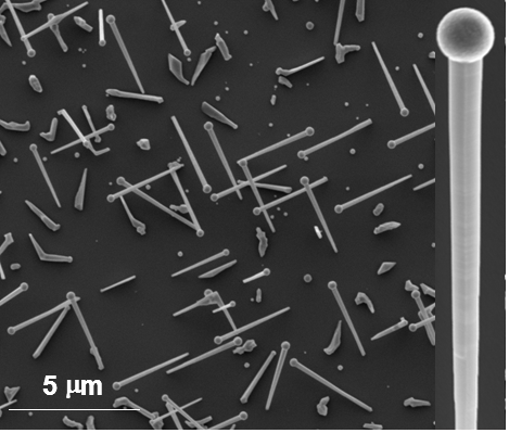
In this work we focus on optical properties of GaAs:Mn NWs measured by photoluminescence (PL), cathodoluminescence (CL) and micro Raman scattering (μ-RS). The NWs were grown in self-catalytic growth mode on oxidized Si(100) surface by MBE and characterized by SEM, TEM, and electron transport measurements. In order to analyze the influence of Mn on the physical properties of NWs the undoped GaAs NWs obtained in otherwise exactly the same manner as those containing Mn were also investigated. The NWs are quite uniform in terms of sizes (diameters and lengths being close to 150 nm and 5 μm, respectively) – see Figure 1. A slight decrease of the NW diameter with an increasing distance from the NW top can be noticed. 
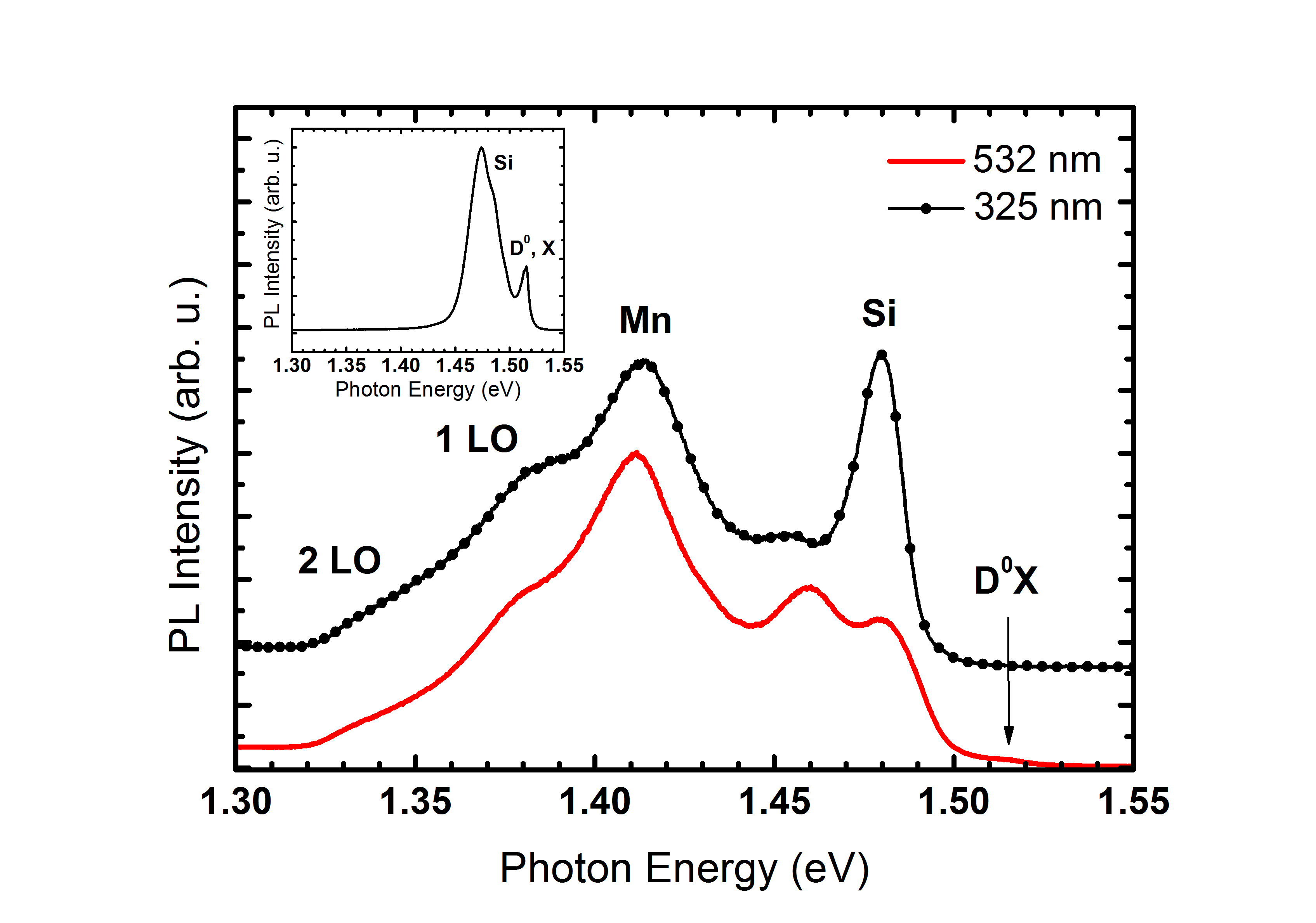
Figure 1. Scanning electron microscopy images of GaAs:Mn nanowires grown on Si(100).  Figure 2. Low temperature PL spectra (normalized to the highest intensity) for GaAs:Mn NWs at different excitations (532 nm and 325 nm laser lines). The inset shows the low temperature PL spectrum of GaAs NWs at excitation of 532 nm laser line. Figure 2. Low temperature PL spectra (normalized to the highest intensity) for GaAs:Mn NWs at different excitations (532 nm and 325 nm laser lines). The inset shows the low temperature PL spectrum of GaAs NWs at excitation of 532 nm laser line.
The comparision of PL spectra measured for GaAs and GaAs:Mn NWs is presented in Figure 2. The transitions related to the Si impurities, introduced into NWs from the substrate during the growth, are present both in undoped and Mn-doped NWs. In the latter case a transition at 1.41 eV associated with Mn acceptor states was also detected. This is a direct proof that the Mn2+ acceptors are located at Ga sites of the GaAs host lattice of the NWs. CL measurements performed on the single NW proved definitely that the PL signal came from the NWs only, not from the sample surface between them. An anomalous temperature dependence of the exciton emission was also found for GaAs:Mn NWs and explained by the thermal activation of Mn acceptor states. The μ-RS spectra, taken for the single NW revealed that the Mn concentration in GaAs:Mn NWs should not exceed 0.05% (1•1019 cm-3). This value is much lower than the Mn/Ga flux ratio (about 3%) applied during the MBE growth. For both GaAs and GaAs:Mn the structures resulting from surface optical phonon modes were also found. The results of resistivity measurements as a function of temperature showed that contrary to undoped GaAs NWs the Mn doped ones are conductive. The p-type of this conductivity confirms the acceptor character of Mn impurities embedded into NW. The direct evidence that a substantial accumulation of Mn takes place inside the catalyzing Ga droplets at the top of the nanowires only was also found by TEM investigation. |
| Legal notice |
|
| Related papers |
Presentation: Oral at 17th International Conference on Crystal Growth and Epitaxy - ICCGE-17, Topical Session 2, by Katarzyna GasSee On-line Journal of 17th International Conference on Crystal Growth and Epitaxy - ICCGE-17 Submitted: 2013-04-15 22:10 Revised: 2013-05-01 22:21 |