| Search for content and authors |
Optimization of technology for contact metallization in electronic devices - XRD and EXAFS studies |
| Krystyna Lawniczak-Jablonska 1, Marcin T. Klepka 1, Anna Wolska 1, Elzbieta Dynowska 1, Michał A. Borysiewicz 2 |
|
1. Polish Academy of Sciences, Institute of Physics, al. Lotników 32/46, Warszawa 02-668, Poland |
| Abstract |
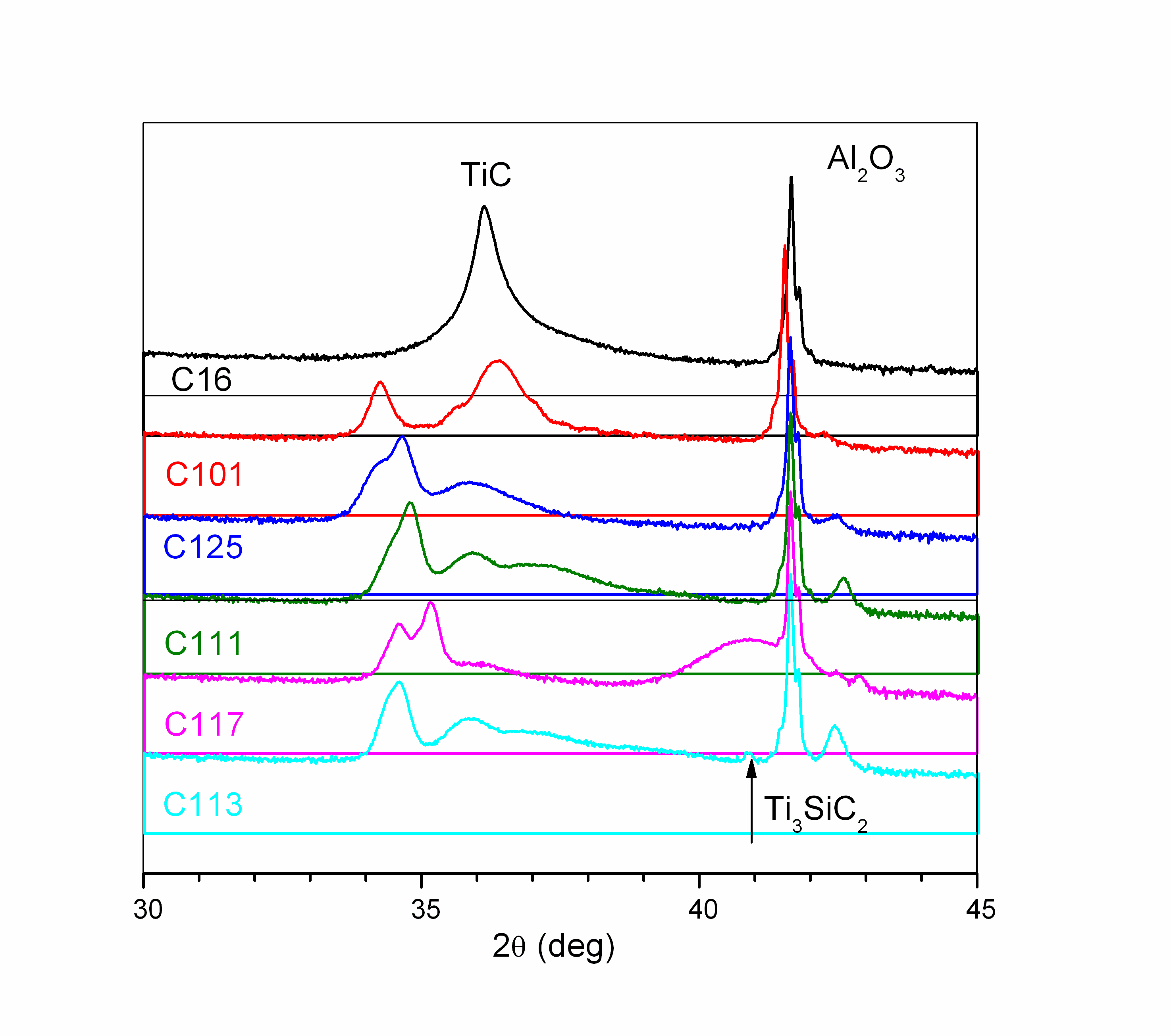
Semiconductor III-N based High Electron Mobility Transistors (HEMT) used for high frequency and high power applications require thermally and chemically stable metallization. The high current-induced heat dissipation in the metallization adds to the environmental heat of such devices, leading to fast degradation of the conventional Ti/Al ohmic and Ni/Au Schottky contacts. The unique combination of metallic electro-thermal conductivity with the ceramic resistance to oxidation and thermal stability makes the ternary compounds belonging to MAX phases in particular the Ti3SiC2 phase, promising as the materials potentially applicable for metallization in such electronic devices. Most of the papers discussing the fabrication of the MAX compounds are related to the synthesis of bulk compounds from powders. Only recently there have been reports on the growth of thin film MAX phases using physical vapour deposition, in particular by means of high-temperature magnetron sputtering. The performed studies aimed at the development of materials for applications in metallization with improved thermal ability. The work focused on synthesizing thin monocrystalline films of Ti3SiC2 by means of high-temperature magnetron sputtering. The studies were performed on layers grown by sputtering from Ti, C and Ti-Si-C composite targets and by sputtering form three targets (Ti, C and Si). In the first case the influence of C content in the TiC buffer layer on the crystal structure of Ti-Si-C layer grown from compositional target is reported. In the second case the influence on the stoichiometry of the formed phases, changes of the power applied to the different targets is discussed. Although Ti3SiC2 is the most studied among the MAX phases, there are no reports focused on the mechanisms of thin-film formation at the atomic level. The characterization of the layers was performed by X-ray diffraction methods (XRD) and subsequently by X-ray absorption (XAS). In most of the cases the XRD studies showed many disagreements with the assumed long range crystalline order. Therefore, the XAS an atomic sensitive probe was applied as the most suitable technique to examine the atomic order around Ti atoms. The XRD for layers grown for the series of samples with different power applied for three independent targets are presented in Fig. 1. One can notice that the shape of the diffraction pattern is changing depending on the applied power. However, only in case of samples marked as C113 and C117 the peak (small and sharp and high and broad, respectively) which can be related to Ti3SiC2 phase was detected.
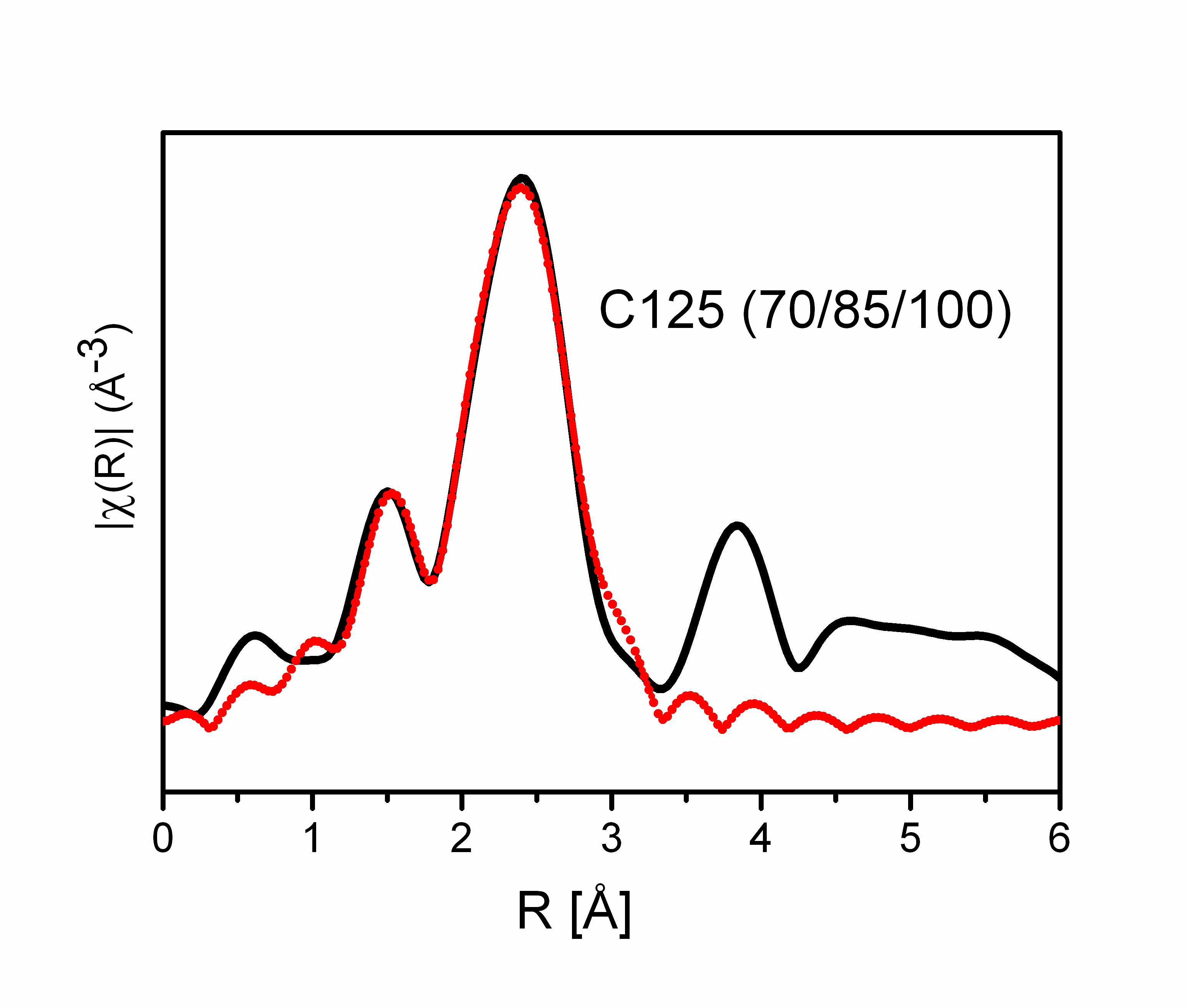
Figure 1. The XRD results for samples produced with different power at three targets. The diffraction peaks from the Al2O3 substrate, TiC compound and position of reflection for Ti3SiC2 are indicated. It can be concluded from the performed XAS studies that the creation of the local atomic order around Ti atoms similar to the Ti3SiC2 phase was observed but not all atomic positions are fully occupied: (i) at carbon atoms position, where 3.6 atoms should be located, there are about 1 ÷ 2 vacancies; (ii) in case of silicon, instead of 1.2 atoms there are almost 3 atoms and 6 in the case of the C125 sample. It indicates that some other phase (like TiSi2) coexists with the MAX phase; (iii) there is a lack of Ti atoms in all the MAX like phases produced - at the distance 2.99 Å and 3.09 Å there should be 4.8 and 6 Ti atoms, respectively. XAS analysis showed only 3 ÷ 5 Ti atoms in both positions together. The example of modelling for sample C125 is shown in Fig.2. In the case of samples grown from the three elemental targets many vacancies in the position of C and Ti were also detected. The crystallographic phases found by XRD cannot be unambiguously ascribed to the known crystal structures.
Figure 2. The magnitude of Fourier transformation of EXAFS oscillations for the C125 sample (black line) and fit to the model (red -dotted line). The numbers in the brackets denote the power fed to the Ti/Si/C targets respectively. The performed EXAFS analysis led to the following conclusions for the technological processes. The power fed to produce the Ti3SiC2 stoichiometry (MAX phase) in the grown layers was considerably too low at the Ti and C targets. In the case of Si target the power fed was too high, that led to the TiSi2 – like phase formation. Moreover, the changes of power fed to C and Si targets did not influence the number and positions taken by these atoms. Acknowledgements: Research in part financed by the European Union within the European Regional Development Fund- project InTechFun. The measurements performed at synchrotron have received funding from the European Community's Seventh Framework Programme (FP7/2007-2013) under grant agreement n° 226716. |
| Legal notice |
|
| Related papers |
Presentation: Poster at IX Krajowe Sympozjum Użytkowników Promieniowania Synchrotronowego, by Krystyna Lawniczak-JablonskaSee On-line Journal of IX Krajowe Sympozjum Użytkowników Promieniowania Synchrotronowego Submitted: 2011-05-30 09:45 Revised: 2014-10-06 14:03 |