-
Overview
-
Topics
- E-MRS Fall Meeting 2006 homepage
- Invited talks of Plenary session
- Nanostructured composite films: synthesis, characterization, properties, and applications
- Nanomaterials in catalysis
- Doped nanopowders: synthesis, characterisation, applications
- Polymer materials modified by nanoparticles
- Dilute magnetic materials for spintronic applications
- Wide Band Gap II-VI Semiconductors: Growth, Characterization and Applications
- Multiscale kinetic modelling of materials
- Phase Diagrams, Phase Stability: Theory and Applications
- Surface functionalization and activation of biomaterials
- Complex oxide materials for new technologies
- Following companies welcome you at their booth
-
Satellite events
-
Register
- Registration and abstract submission closed
- Book of abstracts
- On-line timetable
- Event statistics
- On-line journal
-
Archives
Welcome
Notice:
In order to your company data (name, address and profile) have been placed in Book of Abstracts (BoA), please fill in the registration form on the EMRS Fall Meeting website.
http://www.e-mrs.org/meetings/fall2006/
- Click on the Registration and abstract submission
- Create new account
- Each person who will be your company representative should register himself separately (for delivering badges)
- From the list of interests choose "exhibition" and place your company description in the abstract window (for placing your company data in BoA) - it should be done by one of registering representatives only!
Location, dates and hours
The exhibition will be held from 4
th-8
th September 2006 and will coincide with the technical
programme of the Meeting. The exhibition space will be located in the
Main Hall of the Warsaw University of Technology.
Address: Plac Politechniki 1, 00-661 Warsaw,
Poland.
Monday 4th – Thursday 7th |
Friday 8th |
09:00 am – 05:00 pm |
9:00 am – 1:00 pm |
Installation & Dismantling
The arrangement of the booths will be organised by the WUT. The
exhibitors will be informed of the exact location of their boots
one week before the exhibition start.
The boots will be available for exhibitors from
9am
on Monday, September the 4
th. Considering the Conference programme
it is not possible to arrange booths earlier. Dismantling
the booth:
Friday, September 8
th, by 3pm.
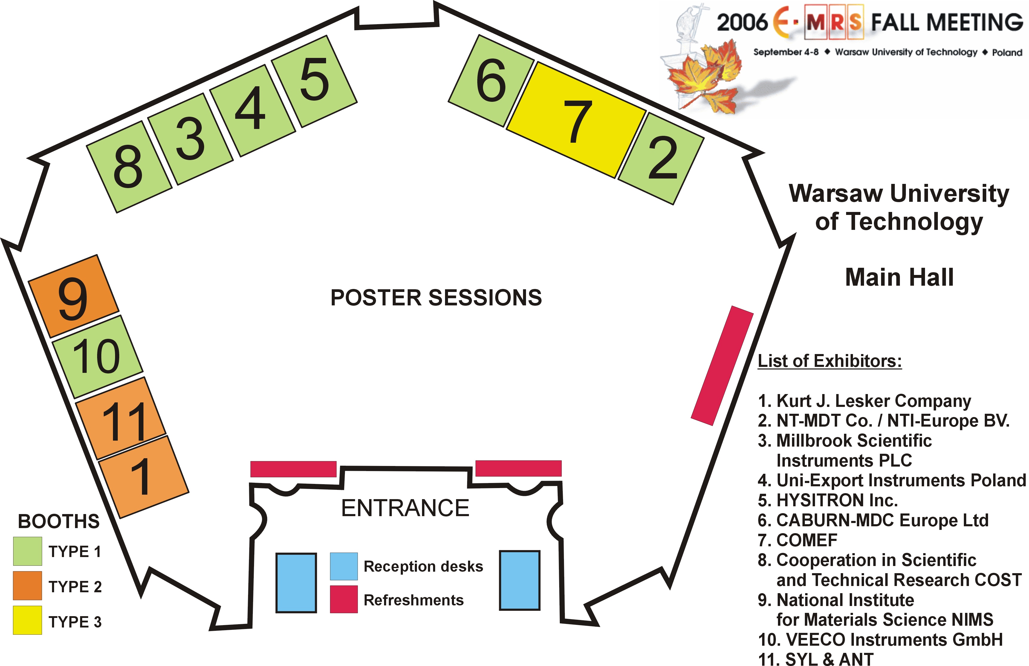
NOTE! We are introducing final booths arrangement

E-MRS Fall Meeting 2006 Exhibitors

10025 Valley View Rd.
Minneapolis MN 55344 USA
Phone: +1 952 8356366
Fax: +1 952 8356166
Hysitron is a leading manufacturer of nanomechanical test instruments for the materials research scientist. Tests include nano-hardness, fracture toughness, elastic modulus, stressstrain, friction, wear and scratch resistance of bulk materials, ultra-thin films, electrical resistance during indentation, nanostructures (MEMS), and nanocomposites. Hysitron 's family of nanomechanical test instruments includes the TriboIndenter® comprehensive test system, TriboScope® interfaced to commercial AFM's, the Ubi 1® dedicated scanning nanoindenter; the nanoECR™ for simultaneous electrical measurements, and the nanoTensile™ 5000. All Hysitron indentation instruments offer proprietary SPM imaging, allowing pre- and post-test in-situ imaging. Advanced features such as quantitative mapping of modulus, dynamic testing (nanoDMA II ™), and acoustic emission monitoring during nanoindentation are available.
________________________________________________________________________________
 NT-MDT Co./NTI-Europe BV.
Arnhemseweg 34d
7331 BL Apeldoorn
The Netherlands
Phone: +31 55 540 2565
Fax: +31 55 540 2566
NT-MDT Co
is working as instrument maker and solution provider in the fast
area of Nano Technology and research.
As selected member of the Dutch Polymer Institute (the largest
European merge of science and industry in Polymers Research) special
equipment has been developed for virtually any nano-scale imaging and
manipulation task. Any variable environment can be created and
controlled. Up to 40 different analysis types range from atomic scale
to about 150 micro meter.
Worlds best results in nano lithography have been obtained with
the solutions delivered by
NTI-Europe BV.
________________________________________________________________________________
COST
European
 Cooperation in Scientific
and Technical Research
Avenue Louise 149
1050 Brussels
Belgium
Phone: +32 2 533 3800
Fax: +32 2 533 3890
Founded in 1971,
COST
is an intergovernmental framework for
European Co-operation in the field of Scientific and Technical
Research, allowing the co-ordination of nationally funded
research on a European level.
COST
Actions cover basic and pre-competitive research as well as
activities of public utility.
The goal of
COST
is to ensure that Europe holds a strong position in the field of
scientific and technical research for peaceful purposes, by
increasing European co-operation and interaction in this field.
To emphasise that the initiative came from the scientists and
technical experts themselves and from those with a direct interest in
furthering international collaboration, the founding fathers of
COST
opted for a flexible and pragmatic approach.
COST
activities have in the past paved the way for Community
activities and its flexibility allows
COST
Actions to be used as a testing and exploratory field for
emerging topics.
The member countries participate on an
"à la carte" principle and activities are launched on a
"bottom-up" approach. One of its main features is its built-in
flexibility. This concept clearly meets a growing demand and in
addition, it complements the Community programmes.
COST
has developed into one of the largest frameworks for research
co-operation in Europe and is a valuable mechanism co-ordinating
national research activities in Europe. Today it has almost 200
Actions and involves nearly 30,000 scientists from 34 European member
countries and more than 80 participating institutions from 11
non-member countries and Non Governmental Organisations.
________________________________________________________________________________
National Institute for Materials Science
![]() 1-2-1 Sengen
1-2-1 Sengen
305-0047 Tsukuba
Japan
Phone: +81 029 859 2494
Fax: +81 029 859 2400
The National Institute for Materials Science (NIMS) was established with the overall purpose of improving the level of material science and technology by conducting research and development work in a comprehensive manner, including basic research in material science/technology and R&D in connection with associated technologies and the research and intellectual infrastructure. NIMS is pleased to introduce these publishing output for a community in materials science research.
NIMS has also strengthened to publish information of materials science, "Science and Technology of Advanced Materials (STAM)". The journal comprises full papers and review papers, and the Editorial Board consists of 30 specialists worldwide. STAM covers theoretical analysis, synthesis and processing, phase and structure analyses, characterization, properties, engineering and applications ."Materials Science Outlook", which identifies and analyzes trends in policies, measures, and research related to materials science both within and outside Japan. This book series are intended for policy makers, research institute managers, and materials science researchers both domestic and overseas."e-materials.net" for scientists in materials science. This site is designed to support communication such as information exchangeing among scientists, and is supported by several institutes, universitied and academic societies in Japan.- Shared use of institute facilities and equipment with researchers from other institutions.- Encouragement of practical application of R&D results, including transfer to the private sector.- Basic research related to material science and technology, and research and development ofrelated research and intellectual infrastructure.
________________________________________________________________________________
COMEF Aparatura Naukowo-Badawcza
 Kalinowa 41
40-750 Katowice
Phone: +48 32 2034149
Fax: ex.30
COMEF is representing in Poland leading French, Japanese, American, Danish and German producers of scientific and research equipment.
We offer equipment, full service and technical advice concerning methods of measurement.
Firma COMEF reprezentuje w Polsce czołowych producentów aparatury naukowo-badawczej oraz kontrolno-pomiarowej .
ADIXEN ( ALCATEL)pompy próżniowe: bezolejowe, olejowe, Rootsa,
turbomolekularne oraz helowe wykrywacze nieszczelności, mierniki
próżni i szeroki asortyment podzespołów
ANTON PAARmikrofalowe systemy do przygotowywania próbek oraz
do syntezy związków organicznych (mineralizatory mikrofalowe)
CALIFORNIA ANALYTICAL INSTRUMENTSanalizatory gazów: CO, CO2,
NOx, SO2
CAMECAmikrosondy jonowe SIMS magnetyczne i kwadropulowe,
mikrosondy elektronowe
CLIMATS SAPRATIN komory: klimatyczne, solne, temperaturowe,
szoku termicznego
CRESSINGTON napylarki do napylania węglem oraz metalami
DANSENSOR przemysłowe mierniki O2 i CO2, analizatory gazów
on-line, miksery gazów, próżniowe wykrywacze nieszczelności,
analizatory przepuszczalności, analizatory MAP
DIGITAL DATA SYSTEMS bomby kalorymetryczne
GORATECaparatura do pomiaru i analizy promieniowania
podczerwonego, bezkontaktowy pomiar temperatury, kamery termowizyjne
GV INSTRUMENTS spektrometry masowe
HITACHI mikroskopy elektronowe: skaningowe, transmisyjne, STEM
HORIBA analizatory węgla i siarki, analizatory azotu tlenu i
wodoru, granulometry, analizatory oleju w wodzie, mierniki jakości
wody, analizatory XRF, analizatory siarki w paliwach
JOBIN YVON siatki dyfrakcyjne, monochromatory, elipsometry,
spektrofluorometry, spektrometry: ICP, GDS, ISKROWE, RAMANOWSKIE
MTS NANO INSTRUMENTS nanotwardościomietrze, scrach testery
NEWPORT elementy optyczne, optyka światłowodowa, siatki
dyfrakcyjne, filtry optyczne, stoły optyczne, układy
mikromechaniczne, układy opto-mechaniczne, itp..
ORIEL monochromatory, źródła światła, lampy kalibracyjne,
oświetlacze, symulatory świata słonecznego, spektrometry FT-IR
PSIA mikroskopy sił atomowych
RIBER komponenty UHV, systemy MBE
QUESANT mikroskopy sił atomowych
SECOMAM spektrofotometry, analizatory wody i ścieków,
analizatory biochemiczne
SETARAM kalorymetry (CALVET, DSC), dylatometry
wysokotemperaturowe, analizatory termiczne (TG, TG-DTA, TGA-MS,
TG-FTIR)
SPECTRA PHYSICSlasery: gazowe, na ciele stałym (YAG),
pikosekundowe, femtosekundowe, wzmacniacze optyczne
THERMAL TECHNOLOGY INC piece: wysokotemperaturowe, próżniowe,
ciśnieniowe, laboratoryjne
WALTER- BAI uniwersalne maszyny wytrzymałościowe, pełzarki
Prowadzimy również pełny serwis oferowanych przez nas urządzeń oraz szkolenia w zakresie ich obsługi.
________________________________________________________________________________
 Caburn-MDC Europe Ltd
12 Horsted Square
Bellbrook Business Park
Uckfield, East Sussex
TN22 1QG
United Kingdom
Welcome to Caburn-MDC Europe Ltd , exclusive European distributors for both MDC Vacuum Corporation and Insulator Seal Incorporated. We are working together to provide one of the most extensive ranges of high- and ultra-high vacuum components to scientists throughout Europe.
From basic flanges to innovative valves, feedthroughs and deposition equipment, our comprehensive online catalogue can provide you with details on a wide range of standard products, all fully specified and priced online. Many of our products are available for rapid delivery.
________________________________________________________________________________
 UNI-EXPORT INSTRUMENTS Polska
ŻURAWIA 6/12,
00-503 WARSZAWA
Phone: +48 22 6268786
Fax: +48 22 6268785
We are authorised representative of leading
manufactures and suppliers of research equipment. We offer technical
support and service for wide range of instruments dedicated for
various applications.
Our product range includes:
- instruments for measurements of surface area and porosity,
density and adsorption of gases,
- equipment for stability control of dispersions, monitoring of
drying and curing properties of film-forming products,
- scanning electron microscopes and accesories,
- hardness testers, optical emmision spectrometers,
- ultrasonic cleaners, dewards,
- software for image analysis and 3D
reconstructions/measurements of surface.
________________________________________________________________________________
 MILLBROOK SCIENTIFIC INSTRUMENTS PLC
Blackburn Technology Centre,
Challenge Way,
Blackburn,
Lancashire,
BB1 5QB,
United Kingdom
Tel: +44 (0)1254 699606
Fax: +44(0)1254 699610
http://www.millbrook-instruments.com
Millbrook Scientific Instruments plc supplies a range of equipment for the measurement of mechanical, optical and chemical nanoscale properties of solid surfaces.For chemical surface analysis the Millbrook MiniSIMS uses Secondary Ion Mass Spectrometry (SIMS) to provide detailed chemical information from just the topmost atomic layers of substrate surfaces such as glasses, metals or plastics or of thin films and coatings applied to them.
Today, the MiniSIMS is being used worldwide in R&D, quality control and failure analysis roles in industries and university departments encompassing a wide variety of sectors and disciplines from biomaterials to electronics. As well as checking for surface contamination the miniSIMS can determinate the uniformity of a coating or the effectiveness of a surface modification process. In profiling mode, the primary ion probe can remove material during analysis allowing chemical information to be acquired as a function of depth. Combined with the mapping facility provided by focussing and scanning the probe, a complete 3D chemical characterisation of the solid can be obtained. Furthermore, the use of mass spectrometry means that the instrument can not only detect all the elements, but can also identify the structure of organic species.
In stark contrast to traditional UHV surface analysis instruments, the miniSIMS is relatively low cost, compact and portable, fitting nearly on top of an average-sized desk. The instrument can typically perform a complete analysis within 15-20 minutes, and an operator can be trained to use it in a day. Worldwide remote control over the internet/modem connection adds further value to multi-site portability.
Optical properties can be measured by the Aquila ‘nkd’ spectrophotometer range which is capable of high precision, non destructive analysis of film thickness, refractive index index and absorption for single and multi-layer nanoscale films on both transparent and absorbing substrates.
A complete nano-mechanical testing solution is provided by the Micro Materials nanoTest system, which as well as nanoindentation and nano-scratch at ambient or high temperatures can perform measurements for study of nano-wear and dynamic nano impact testing.
________________________________________________________________________________
 KURT J. LESKER
Company
16 Ivyhouse Lane
Hastings, East Sussex
TN35 4NN, England
Phone: 44-1424-719101
Fax: 44-1424-426233
COMPANY PROFILE:
KJLC is a world class manufacturer
& distributor of high and ultra-high vacuum components and thin
film deposition systems, used by university, government, and
industrial R & D facilities; OEMs; semiconductor processors;
industrial vacuum coaters; and others in thin film deposition market
segments.
TECHNICAL CAPABILITIES:We have in-house design, engineering and manufacturing capabilities for a large range of projects (beamline components, space simulators, complex manipulators, complete deposition systems, etc)
EXPERIENCE:We have supplied vacuum components (including valves, special feedthroughs fabricated items) to most of the government labs across Europe and North America
SPECIFIC EXPERTISE:
UHV technology, sample manipulation & transfer, manufacture
of stainless steel products (chambers, specials, sub assys),
distribution of complete range of vacuum products
DESIGN & MANUFACTURING:
AutoDesk Mechanical Desktop & Solid Edge modelling
software; ISO9001 accredited
RESEARCH & DEVELOPMENT CAPABILITIES:Various alliances with Universities in UK & USA for R&D work
PRODUCTION FACILITIES:UK manufacturing base in Hastings,
Sussex, UK
75,000 sq ft production facility in Pittsburgh, USA
________________________________________________________________________________
 VEECO Instruments GmbH
Dynamostr. 19
68165 Mannheim, Germany
(49) 621 842 10 0
(49) 621 842 10 22
Veeco Instruments’ metrology and process equipment products provide solutions for nanoscale applications in the worldwide LED/wireless, data storage, semiconductor and scientific research markets. Veeco is the world’s leading supplier of equipment to the compound semiconductor industry.
Our Metrology products are used to measure at the micro- and nanoscale, and include atomic force microscopes, scanning probe microscopes, and stylus and optical profilers.
Our Process Equipment tools help create nanoscale devices and include molecular beam epitaxy (MBE), metal organic chemical vapour deposition (MOCVD), ion beam etch and deposition, physical vapour deposition, precision lapping and dicing technologies. VEECO is the only company that offers both MBE and MOCVD tools, and provides both research and production solutions for a wide variety of applications and emerging materials.
Veeco’s complementary processing and metrology tools, plus its Process Integration Center, give customers the most complete one-stop portfolio of compound semiconductor equipment.
________________________________________________________________________________
 SYL & ANT Instruments
ul. Pyskowicka 12
44-172 Niewiesze, Poland
(+48) 32 2303201
(+48) 32 2303301
SYL & ANT Instruments was founded in 1992 as a continuation of the Bureau of Technical Information (since 1986). The company is situated in Niewiesze near Gliwice, some 3 km away from the A4 motorway exit, direction Pyskowice.
The company was founded by Josef Nitka, engineer, author and co-author of 7 patents and 75 utility models, prize-winner of inventors competitions, one of two representatives of the Polish Academy of Sciences at the first World Exhibition of Young Inventors (1985), member of NOT-Technical Associations and one of founders and members of the elitist Association of Polish Consultants.
The goal of our activities is solving analytical problems of our customers with the aid of modern, although often hardly known in Poland, but worldwide recognised analytical and measuring equipment. We use our vast practical experience in the area of laboratory analysis.
We are pioneers in introducing the newest and best word instrumentation for the trace analysis of nitrogen , sulphur, chlorine compounds, automated chemical and petrochemical analyzers, granulometry , porosity, microporosity and surface area measurements, laboratory autoclave systems as other applications on the Polish market.
We represent renowned foreign manufacturers on the Polish market.
Autoclave Engineers, Calibrage, CMC, ThermoEuroglas, Taylor-Wharton-Harsco, Iatron Lab., Mercury Instruments, Micromeritics, MTS GmbH Sy-Lab, Konica-Minolta,
Generally we supply our instruments and service directly as well as through our dealers in the whole area of Poland, but we servicing our Clients in the other part of Europe, also.
________________________________________________________________________________
 A.P. Instruments
ul. Jaworowa 32/2;
02-798 Warszawa
tel. 022-355-3561 fax: 022-355-3562
e-mail: [email protected]
A. P. Instruments przedstawiciel firmy Malvern Instruments, Sieverst; urządzenia pomiarowe
________________________________________________________________________________
Exhibition Coordinator
Grzegorz Wojas
Warsaw University of Technology
Faculty of Materials Science and Engineering
141 Wołoska St.; 02-507 Warsaw, POLAND
e-mail:
[email protected]
NEW NUMBER
Phone/fax
: (+48 22) 6608108
Fax: (+48 22) 6608750 (WUT office)
