| Search for content and authors |
Evolution of threading screw dislocation conversion during solution growth of 4H-SiC |
| Shunta Harada , Yuji Yamamoto , Kazuaki Seki , Atsushi Horio , Takato Mitsuhashi , Miho Tagawa , Toru Ujihara |
|
Department of Materials Science and Engineering, Nagoya University, Furo-cho, Chikusaku, Nagoya 464-8603, Japan |
| Abstract |
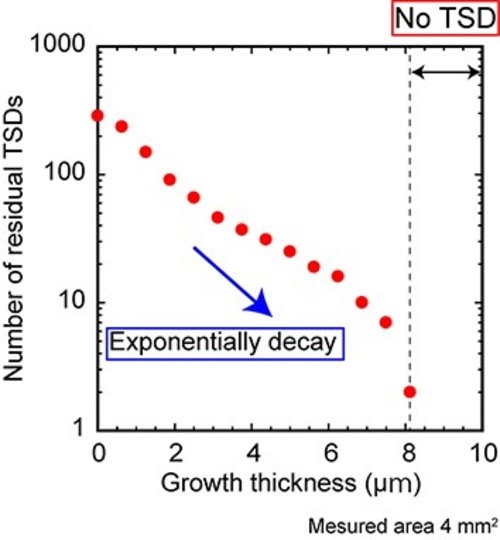
| Silicon carbide (SiC) is a promising material for next-generation power device because of its excellent physical properties. For high-performance SiC power devices with long-term reliability, the improvement of crystal quality is essential. Solution growth has an advantage to grow high quality crystals because the condition is close to thermal equilibrium. Recently, we have revealed that threading screw dislocations (TSDs) in seed crystal are efficiently converted into the defects on the basal plane during the solution growth of 4H-SiC. By using the TSD conversion during the solution growth, we have successfully grown high quality 4H-SiC with extremely low TSD density. However, the details of the highly efficient TSD conversion are still not clear. In the present study, we investigate the evolution of TSD conversion during the solution growth of 4H-SiC by synchrotron X-ray topography. Single crystals of SiC were grown on off-axis seed crystals by top-seeded solution growth method. During the solution growth on a vicinal seed crystal, almost all TSDs were converted to the defects on the basal planes by the macrosteps advancing toward step-flow direction as shown in Fig. 1. In the X-ray topography image of the grown crystal, the length of the basal plane defects was different with each other. The length of the basal plane defect is proportional to the depth where the TSD conversion occurs. Therefore the distribution of the defect length indicates that the TSD conversion stochastically take place during the growth. Figure 2 shows the evolution of the residual TSDs with different growth thickness. The TSD density was exponentially decreased and after the 10 micrometer growth there are no TSDs in the measured area corresponding to the TSD density of below 25 cm-2, which is smaller than that of the commercial SiC wafers by two orders of magnitude. Similar TSD conversion has been reported in the epitaxial growth of SiC by chemical vapor deposition (CVD). However, the conversion ratio is as low as 1% in CVD within the growth of about 20 μm. The TSD conversions during CVD were reported to occur only at the interface between substrate and growth layer. On the other hand, the TSD conversions during solution growth intermittently take place during the growth, which leads to the highly efficient TSD conversion. 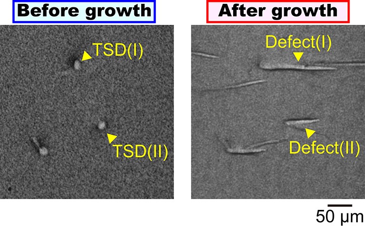
Figure 1. X-ray topography images before and after the solution growth. The length of the Defect (I) and Defect (II) is different, which indicates that the TSD conversions occurred at different depth. |
| Legal notice |
|
| Related papers |
Presentation: Oral at 17th International Conference on Crystal Growth and Epitaxy - ICCGE-17, General Session 7, by Shunta HaradaSee On-line Journal of 17th International Conference on Crystal Growth and Epitaxy - ICCGE-17 Submitted: 2013-03-31 01:29 Revised: 2013-07-19 23:43 |