HVPE-GaN crystallization on non-polar and semi-polar HVPE-GaN seeds will be described. All seeds have been obtained by slicing them from the 5 mm thick HVPE-GaN boule (see Fig.1). This boule was grown in a few subsequent growth runs. The multistep growth process was performed in the following way. First, 500 nm thick MOCVD-GaN on 2 in. sapphire wafer was grown. Then, the template was patterned using a titanium mask. After that, the template was overgrown by the HVPE to a thickness of approximately 1 mm. Then, due to self-separation from the sapphire, a free standing HVPE-GaN crystal was obtained. In the next few steps, such crystal was overgrown by the HVPE to a thickness of about 5 mm. Finally, the HVPE-GaN boule was sliced along non-polar and semi-polar planes. Thus, many substrates in the form of stripes with a few centimeters length and five millimeters width were obtained (see Fig. 2). Their surfaces: (10-10), (11-20), (20-21) and (20-2-1) were prepared to the epi-ready state by mechanical and mechano-chemical polishing. These substrates were used as seeds for the HVPE growth in various directions. Four stripes with four different crystallographic surfaces and c-plane reference substrates were always used as seeds for one HVPE process.. This way, a growth rate and morphology at the same crystallization conditions, but in five crystallographic directions, could be determined and compared. Differences in morphology will be presented in this paper. It will be also shown that the growth rate can be changed more than 10 times (depending on the growth direction) and it can be also varied in the function of carrier gas used in the HVPE process.
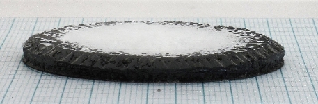
Fig. 1. 5 mm thick HVPE-GaN boule grown in a few subsequent growth runs.
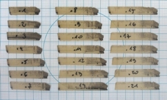
Fig. 2. Stripes sliced from the HVPE-GaN boule with various exposed surfaces: a) (20-21); b) (10-10); c) (11-20); grid line 1 mm.
|