| Search for content and authors |
Heterostructures PbTe:Ga/BaF2/CaF2/Si for IR photodetectors |
| Alexander M. Samoylov 1, Alexandr E. Klimov 2, Aleksey N. Akimov 2, Nikolay S. Paschin 2, Sergey P. Suprun 2, Vladimir N. Shumsky 2 |
|
1. Voronezh State University (VGU), Universitetskaya Sq., 1, Voronezh 394006, Russian Federation |
| Abstract |
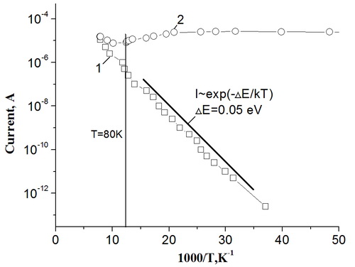
In the present publication, we report data gained in experiments on growing PbTe:Ga films on Si substrates and on examining the properties of In/(p-PbTe:Ga) test photosensitive structures based on such films. The various processes for production of PbTe layers on Si have long been under study (see, e.g. [1]). Advantageous features of such heterostructures include the possibility of fabricating large-format IR photodetectors on individual silicon chips and the possibility of fabricating flip-chip photodetectors, for which matching of multiplexer crystal and FPA substrate in terms of thermal expansion coefficients is not required. Also, experiments on doping PbTe films on BaF2 substrates with gallium were previously reported in the literature [2]. From the standpoint of photodetector applications, the main result obtained in [2] was the revealed possibility of obtaining PbTe films with an extremely low concentration of charge carriers, which, in principle, enables the fabrication of photosensitive structures based on such films. The process used in the present study for growing CaF2/BaF2 buffer layers on (111)-oriented Si substrates was described elsewhere [3]. The Si substrates with CaF2/BaF2 layers used for growing PbTe films on such layers were loaded into the MBE facility in the atmosphere of dry pure nitrogen. The thickness of the PbTe films was about one micrometer. The films were doped with gallium in a gas atmosphere as described in [4]. The source of Ga was Gа0.6Te0.4 alloy. A typical dependence of current on reciprocal temperature in our PbTe:Ga films is shown in Fig.1.
Fig.1. The electric current through a PbTe:Ga/BaF2/CaF2/Si film versus the reciprocal temperature. The sample was shaped as a square, and the bias voltage was U=1.5 V. Curve 1 was measured in the dark, and curve 2, under illumination. The straight line shows an Arrhenius dependence with activation energy ΔE=0.05 eV.
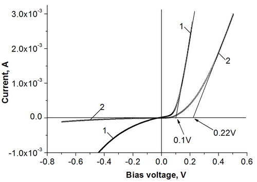
PbTe:Ga films of p-type conductivity with hole concentration p=(1-50)×1012 cm-3 and hole mobility μp>104 cm2 V-1 s-1 at Т=80 K were used. Indium contacts to the samples ranging in area from 75х75 to 1200х1200 μm2 were obtained using thermal evaporation of In in vacuum. Anneals were given to the samples in argon ambient. Measurements were made on non-annealed (Schottky barriers) and annealed (shallow n-p junctions) structures. During measurements, the samples were held at temperature T=80 K in a nitrogen cryostat. The spectral sensitivity of measured structures, generally consistent with the behavior of PbTe photosensitivity in the fundamental absorption region of the material, exhibited interference-induced features, which, in principle, enables optimization of photosensitivity at a desired wavelength through film thickness adjustment. Current-voltage characteristics of a structure 200 μm in diameter measured prior to and after the annealing of the sample in argon atmosphere are shown in Fig.2; during measurements, the structure was shielded from background radiation.
Fig. 2. Current-voltage characteristics of a structure 200 μm in diameter measured prior to (1) and after (2) the annealing of the sample in argon on screening the sample from background radiation. The straight lines show approximations of the linear portions of the characteristics. Approximation of the linear portions of the forward branches of the current-voltage curves has yielded offset voltage values 0.1 V and 0.22 V, which can be identified as the diffusion potential values for Schottky barriers and n-p junctions (before and after annealing of the samples). Photosensitivity and noise measurements performed under low background illumination conditions have yielded for the maximum detectivity a value D*>1011 W×cm×Hz-0.5. Charge transport mechanisms in the films and available potential for improving characteristics of the photodetectors and for use of obtained film structures in the development of FPA photodetectors on silicon chips are discussed. This work was supported by the Ministry of Science and Education of the Russian Federation under Grant No. 2012-1.1-12-000-2003-120.
References 1. C. Maissen, J. Masek, H. Zogg, S. Blunier. Appl. Phys. Lett. 53, 1608 (1988). 2. B.A. Akimov, V.A. Bogoyavlenskii, L.I.Ryabova, et al. Phys. Rev. B 61, 16045 (2000). 3. S.P. Suprun, and D.V. Shcheglov. JETP Letters 88, 365 (2008). 4. L.F. Vasil’eva, A.E. Klimov, N.I. Petikov, and V.N. Shumsky. Inorganic Materials 37, 144 (2001).
|
| Legal notice |
|
| Related papers |
Presentation: Poster at 17th International Conference on Crystal Growth and Epitaxy - ICCGE-17, General Session 10, by Alexander M. SamoylovSee On-line Journal of 17th International Conference on Crystal Growth and Epitaxy - ICCGE-17 Submitted: 2013-04-13 05:34 Revised: 2013-04-15 10:52 |