| Search for content and authors |
Surface morphology and structure of CaF2/BaF2–on-Si epitaxial layers and the electronic properties of the interface with the substrate |
| Alexander M. Samoylov 1, Alexandr E. Klimov 2, Aleksey N. Akimov 2, Nikolay S. Paschin 2, Vladimir N. Shumsky 2, Sergey P. Suprun 2, Evgeniy V. Fedosenko 2, Vladimir G. Erkov 2, Dmitriy V. Scheglov 2 |
|
1. Voronezh State University (VGU), Universitetskaya Sq., 1, Voronezh 394006, Russian Federation |
| Abstract |
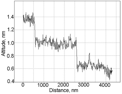
Molecular-beam epitaxy was used to grow layers of alkaline-metal fluorides CaF2 and BaF2 (lattice mismatch values 0.6 and 14%) on (001)- and (111)-oriented Si substrates. In AFM images of the surface of BaF2/CaF2 films on (111)-oriented Si, smooth ordered steps of height (0.4±0.05) nm and length 2 µm were observed (Fig. 1); such steps correspond to half the principal diagonal of the unit cell of BaF2 (0.876 nm).
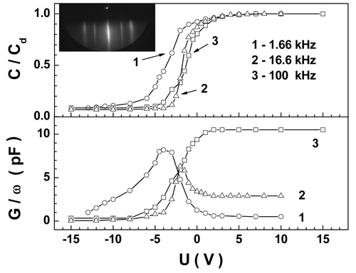
Fig. 1. Surface relief of a BaF2/CaF2/Si (111) structure as measured by a Solver P-47H> (NT-MDT) atomic force microscope. As it was shown in [1], the capacitance-voltage curves of CaF2-on-Si (111) structures proved to be temperature-dependent. The capacitance modulation becomes less pronounced with increasing the growth temperature of the CaF2 layers, and it finally vanishes in samples grown at temperatures above 500°С. Our data and data previously reported by other authors show that, with increase in temperature, for the interfacial region the x-ray photoelectron spectra exhibit a growth of the component due to Si 2p, corresponding to the Si-Ca bond, and a decrease of the component due to the Si-F bond. A similar tendency in the evolution of the physico-chemical interfacial structure was also observed for BaF2 layers grown on Si (001); here, capacitance modulation was observed even in samples obtained at 780°С. In the latter case, the energy density of states at the interface with the substrate was ~1011eV-1cm -2, and the built-in charge density was (4 to 5)×1011 cm -2 (Fig. 2). Our estimates show that the density of dangling bonds at the interface from the side of Si, which features a shorter lattice constant in comparison with BaF2, reaches ~ 3×1014cm-2, the misfit dislocations forming a dislocation network with a step of 3 nm. Thus, the explanation to the observed correlation between the built-in charge and the physico-mechanical structure of the heterointerface proposed in [1] for CaF2/Si structures turns out to be inappropriate for BaF2/Si structures. Moreover, the difference by three orders between the density of Si dangling bonds at the BaF2/Si interface and the density of electron states determined from measured C-V and G-V characteristics of the samples makes the correlation between the indicated quantities doubtful.
Fig. 2. С-V characteristics (upper panel) and G-V characteristics (lower panel) of BaF2-Si(001) MIS structures measured at three frequencies. The inset shows a reflection electron diffraction pattern obtained on exposing the surface of the BaF2-on-Si(001) film to fast electrons. The spatial period of the misfit dislocation network is close to the size of the cells formed as a result of 7×7 reconstruction of the Si (111) surface, such reconstruction being accompanied by transformation of the Si (111) surface electronic structure. It can be hypothesized that spatially ordered defects present in the samples in a high density could also form a quantum subsystem “deactivating” the interfacial states. In principle, the electron states in the system may appear superimposed upon one of the allowed bands of Si, and they therefore can escape detection with standard observation means [2]. Also, we examined the influence which the diffractometer electron beam had on the growth and morphology of CaF2 and BaF2 layers. It was shown that electron-beam irradiation leads to formation of voids in the material. The size and density of the voids depended on the irradiation dose, thus being defined by the integral beam charge falling onto the sample. The mechanism underlying the formation of voids in the material involves, first, the beam-induced decomposition of the material and fluorine desorption in it and, second, the loss of positively charged metal ions in the material caused by their drift escape from the region to which the negative charge due to fast electrons sank [3]. References 1. C.-C. Cho, T.S. Kim, B.E. Gnade, H.Y. Liu, Y. Nishiokaa, Appl. Phys. Lett. 60, 383 (1992). 2. S.P. Suprun, D.V. Shcheglov, JETP Letters 88, 365 (2008). 3. S.P. Suprun, V.G. Kesler, E.V. Fedosenko, Observation of chemical reactions in solid phase using X-ray photoelectron spectroscopy, in: “Stoichiometry and Materials Science - When Numbers Matter”, 285-326, InTech, Rijeka, Croatia, 2012. |
| Legal notice |
|
| Related papers |
Presentation: Poster at 17th International Conference on Crystal Growth and Epitaxy - ICCGE-17, General Session 10, by Alexander M. SamoylovSee On-line Journal of 17th International Conference on Crystal Growth and Epitaxy - ICCGE-17 Submitted: 2013-04-12 20:00 Revised: 2013-07-17 22:47 |