| Search for content and authors |
Impact of substrate microstructure on self-induced nucleation and properties of GaN nanowires grown by plasma-assisted MBE |
| Marta Sobanska , Kamil Klosek , Aleksandra Wierzbicka , Jolanta Borysiuk , Slawomir Kret , Giorgi Tchutchulashvili , Sylwia Gierałtowska , Elżbieta Lusakowska , Piotr Nowakowski , Zbigniew R. Zytkiewicz |
|
Institute of Physics, Polish Academy of Sciences, Warsaw 02-668, Poland |
| Abstract |
| Recent in-situ studies of growth of GaN nanowires (NWs) by plasma-assisted molecular beam epitaxy on silicon by Hestroffer et al. [1] show that a massive self-induced nucleation of GaN NWs starts only after partial amorphization of the silicon nitride film that inevitably forms on silicon substrate under nitrogen flux. This result indicates existence of a barrier for GaN nucleation on monocrystalline substrate, so creation of nucleation sites (e.g. by partial amorphization of the substrate) seems to be needed to enhance nucleation rate of GaN NWs. To explore this effect in a more details we have compared efficiency of self-induced nucleation of GaN NWs on three different substrates, namely on bare c-oriented sapphire, on Si(111) with a native silicon nitride layer and on Si(111) coated with a thin amorphous Al2O3 buffer deposited at low temperature by atomic layer deposition. On all substrates catalyst-free growth of NWs proceeded under the same, highly nitrogen-rich conditions at ~750 oC [2]. Comparison of nucleation kinetics by RHEED showed that no NWs nucleation occurred on sapphire. This agrees with observation by Geelhaar et al. [3] who have reported that on the crystalline sapphire NWs do not form under any PAMBE growth conditions. Slow GaN nucleation was observed on partially amorphous silicon nitride film naturally created on the surface of Si(111) due to a high affinity of nitrogen to silicon. Finally, significantly enhanced nucleation of GaN NWs was observed on amorphous Al2O3 buffer. Post growth analysis by scanning and transmission electron microscopy show separated NWs on a bare silicon whereas high density of GaN nuclei are found between NWs grown on Al2O3 buffer (Fig. 1).
This work was partly supported by the European Union within European Regional Development Fund, through grant Innovative Economy (POIG.01.01.02-00-008/08). MS thanks for support from European Social Fund through Human Capital Program and local authorities (Samorząd Województwa Mazowieckiego - „Potencjał naukowy wsparciem dla gospodarki Mazowsza – stypendia dla doktorantów”). [1] K. Hestroffer et al., Appl. Phys. Lett. 100, 212107 (2012). |
| Legal notice |
|
| Related papers |
Presentation: Oral at 17th International Conference on Crystal Growth and Epitaxy - ICCGE-17, Topical Session 3, by Marta SobanskaSee On-line Journal of 17th International Conference on Crystal Growth and Epitaxy - ICCGE-17 Submitted: 2013-04-15 15:44 Revised: 2013-07-23 17:34 |
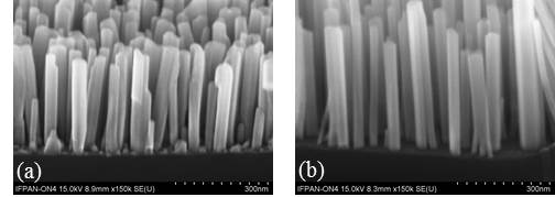 Fig. 1 Cross-section SEM views of GaN NWs (a) on Si(111) substrates with 2 nm thick amorphous Al2O3 buffer and (b) on bare Si(111).