| Search for content and authors |
Growth and properties of inclined GaN nanowires on Si(001) substrates by PAMBE |
| Marta Sobanska 1, Kamil Klosek 1, Jolanta Borysiuk 1, Aleksandra Wierzbicka 1, Krzysztof P. Korona 2, Anna Reszka 1, Zbigniew R. Zytkiewicz 1 |
|
1. Institute of Physics, Polish Academy of Sciences, Warsaw 02-668, Poland |
| Abstract |
| It is well established that self-induced GaN nanowires (NWs) grown by plasma-assisted MBE on bare Si substrates are aligned with the c-axis perpendicular to the substrate surface independently on its crystallographic orientation [1,2]. Such behavior, being different than in other material systems, is due to presence of thin amorphous silicon nitride film that unavoidably forms first at the expense of GaN nucleation and separates GaN NWs feet from Si. In this work we present results of our studies on growth and characterization of GaN NWs on Si(001) substrates. The nanowires were grown under N-rich conditions at ~760oC by plasma-assisted MBE without use of any catalyst. Usually, our growths resulted in a dense ensemble of hexagonal NWs oriented perpendicular to the substrate (Fig. 1a), i.e. aligned in the same way as on Si(111) substrates. However, some samples contained two groups of NWs: vertical and inclined ones (Fig. 1b). 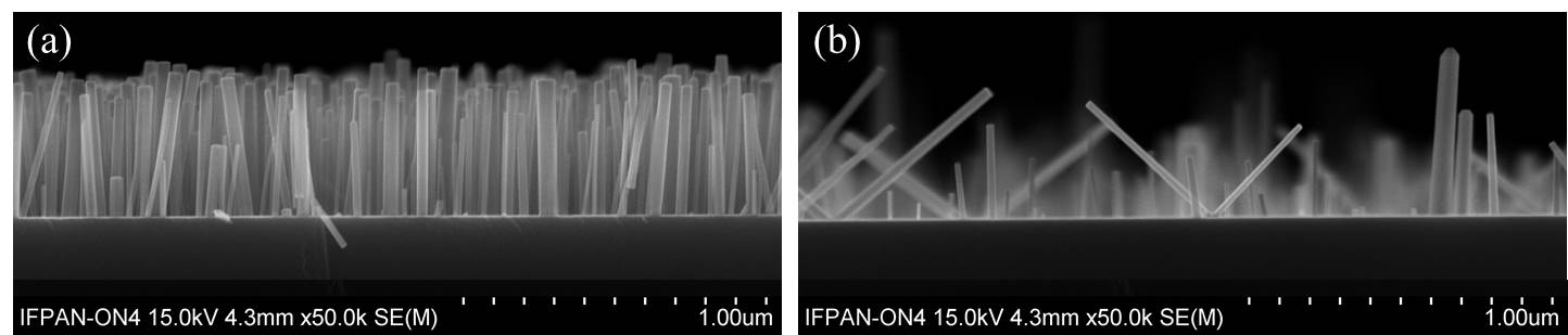
Fig 1: SEM image of GaN NWs on Si(001): (a) standard vertical NWs alone, (b) vertical and tilted NWs. This is unexpected result since to our best knowledge existence of such inclined GaN NWs on Si has not been reported in the literature. While vertical NWs had a typical hexagonal shape, the inclined NWs were slightly more flat. SEM, XRD and TEM studies allowed us to find that the inclined NWs were oriented perpendicular to the (111) planes of Si. HRTEM analysis showed fundamental differences in nucleation mechanisms of the two types of NWs. The vertical NWs were separated from the substrate by ~2 nm thick Si-nitride film (Fig. 2b) as commonly observed in GaN NWs on Si [3]. On the contrary, such film was absent under the inclined NWs, so they nucleated directly on bare Si creating first a zb-GaN nucleus that later on transformed into wurtzite GaN (Fig. 2a). The CBED analysis showed that the polarity of the inclined NWs corresponded to the surface with Ga termination. Low temperature PL and CL studies revealed much more efficient light emission from the inclined NWs than from their vertical neighbors. Finally, we discuss mechanism of formation of inclined NWs as well as methods of controlling the proportion of densities of inclined to vertical NWs. 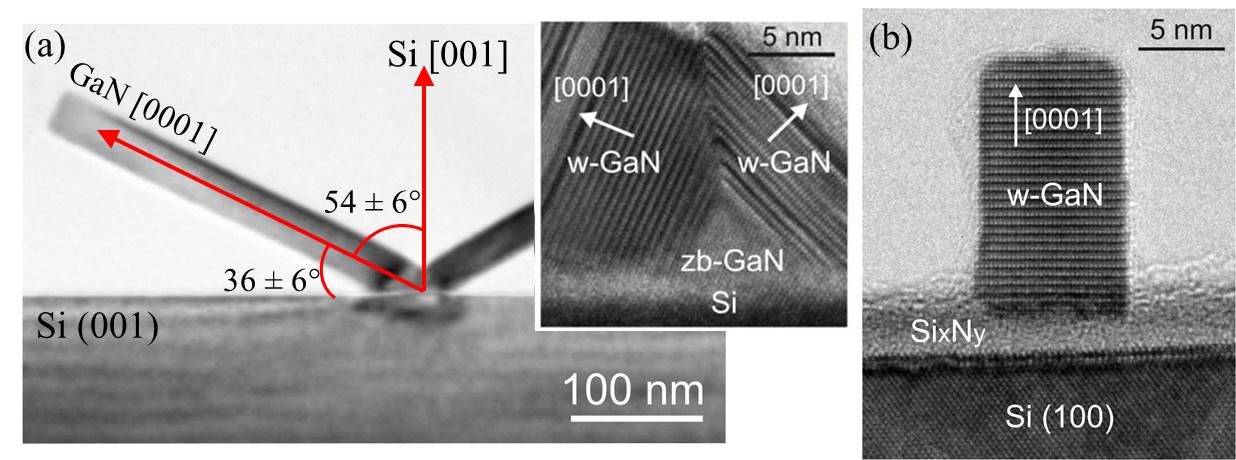 Fig. 2. TEM images of (a) inclined and (b) vertical GaN NWs. Zoomed image in (a) shows zb-GaN nucleus in a direct contact with the Si(001) substrate. This work was partially supported by the European Union within European Regional Development Fund, through grant Innovative Economy POIG.01.01.02-00-008/08 (NanoBiom). MS thanks for support from European Social Fund through Human Capital Program and local authorities (Samorząd Województwa Mazowieckiego - „Potencjał naukowy wsparciem dla gospodarki Mazowsza – stypendia dla doktorantów”). [1] E. Calleja, et al. Phys. Stat. Sol. (b) 244, 2816 (2007). [2] L. Cerutti, et al. Appl. Phys. Lett. 88, 213114 (2006). [3] L. Geelhaar, et al. IEEE 17, 878 (2011). |
| Legal notice |
|
| Related papers |
Presentation: Poster at 15th Summer School on Crystal Growth - ISSCG-15, by Marta SobanskaSee On-line Journal of 15th Summer School on Crystal Growth - ISSCG-15 Submitted: 2013-07-02 09:24 Revised: 2013-07-02 11:26 |