Commercial exhibitionsCommercial exhibitions |
|
Commercial exhibitionsCommercial exhibitions |
|
WUT - EMRS Conference
141 Woloska St. , 02-507 Warszawa, Poland
PEKAO S.A. IV O/Warszawa
IBAN: PL 79124020929522109001000000
SWIFT: PKOPPLPWWA4
Please indicate your company name!
Mo (
Sept. 17)
11:00 – 18:00
Tu (
Sept. 18)
09:00 – 18:00
We
(Sept.19)
09:00 – 18:00
Th (
Sept. 20)
09:00 – 18:00
Fr
(Sept.21) from
09:00 booth dismantling
For detailed information about this events, please click here.
Goods e.g. EQUIPMENT must be delivered/transported to the booth directly by the Exhibitor (Conference Venue – WUT Main Building – Pl.Politechniki 1) and arranged at times other than the official show hours!
FLOOR PLAN for the EXHIBITION
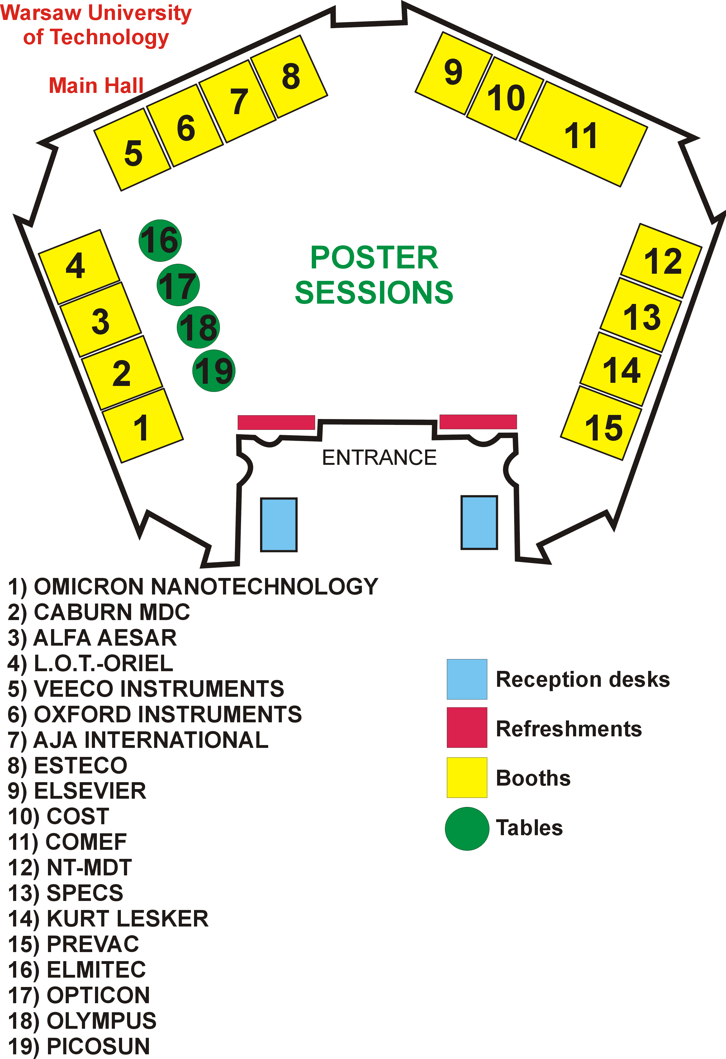
in order of apply
Alfa Aesar GmbH & Co KG
Zeppelinstrasse 7
Postbox 110765
76057 Karlsruhe
Germany
Phone: 0721-84007-260
Fax: 0721-84007-300
E-mail:
[email protected]
Alfa Aesar, a Johnson Matthey Company is a leading international manufacturer and supplier of Research Chemicals, Metals and Materials. With over 27,000 products listed in its catalogue, Alfa Aesar is the single source for customers’ needs for chemicals and materials in sizes for research and scale up. The Alfa Aesar Catalogue carries: Organic compounds, High purity inorganics, Pure elements, alloys, Precious metal catalysts, AA/ICP standards and more.
Alfa Aesar has sales offices and distribution facilities throughout North America, Europe and Asia and a distributor network covering the globe.
___________________________________________________

LOT-Oriel GmbH & Co. KG
Im Tiefen See 58
D-64293 Darmstadt
Germany
Phone: +49 6151 - 88 06 0
Fax: +49 6151 – 896667
E-mail:
[email protected]
LOT-Oriel was founded in 1970 initially as a sales and marketing company for optical components. The abbreviation "L.O.T.” stands for laser, optics and technology, thus outlining the company’s product range. Today, LOT-Oriel is a supplier of equipment and technology in the fields of optical spectroscopy, analytics, laser technology, surface analytics and nanobiotechnology.
One major focus of the company’s nanotechnology activities is the Scanning Probe Microscopy (SPM) in different aspects.
• The Atomic Force Microscope (AFM) from Pacific Nanotechnology features a robust design and easy handling. That allows AFM studies to be carried out alos in routine and quality control,
• Infinitesima overcomes another disadvantage of conventional SPM's, that is the long time needed to aquire an image, With this accessory AFM images can be aquired at video rates.
___________________________________________________

COST
Avenue Louise 149
1050 Brussels
Belgium
Phone: +32 2 5333803
E-mail:
[email protected]
COST- the acronym for European COoperation in the field of Scientific and Technical Research- is the oldest and widest European intergovernmental network for cooperation in research. Established by the Ministerial Conference in November 1971, COST is presently used by the scientific communities of 35 European countries to cooperate in common research projects supported by national funds.
The funds provided by COST - less than 1% of the total value of the projects - support the COST cooperation networks (COST Actions) through which, with only around €20 million per year, more than 30.000 European scientists are involved in research having a total value which exceeds €2 billion per year. This is the financial worth of the European added value which COST achieves.
A “bottom up approach” (the initiative of launching a COST Action comes from the European scientists themselves), “à la carte participation” (only countries interested in the Action participate), “equality of access” (participation is open also to the scientific communities of countries not belonging to the European Union) and “flexible structure” (easy implementation and light management of the research initiatives ) are the main characteristics of COST.
As precursor of advanced multidisciplinary research COST has a very important role for the realisation of the European Research Area (ERA) anticipating and complementing the activities of the Framework Programmes, constituting a “bridge” towards the scientific communities of emerging countries, increasing the mobility of researchers across Europe and fostering the establishment of “Networks of Excellence” in many key scientific domains such as: Biomedicine and Molecular Biosciences; Food and Agriculture; Forests, their Products and Services; Materials, Physics and Nanosciences; Chemistry and Molecular Sciences and Technologies; Earth System Science and Environmental Management; Information and Communication Technologies; Transport and Urban Development; Individuals, Society, Culture and Health. It covers basic and more applied research and also addresses issues of pre-normative nature or of societal importance.
___________________________________________________
 KURT J. LESKER Company
16 Ivyhouse Lane
Hastings, East Sussex
TN35 4NN, England
Phone: 44-1424-719101
Fax: 44-1424-426233
KJLC
is a world class manufacturer & distributor of high and
ultra-high vacuum components and thin film deposition systems, used
by university, government, and industrial R & D facilities; OEMs;
semiconductor processors; industrial vacuum coaters; and others in
thin film deposition market segments.
TECHNICAL CAPABILITIES:We have in-house design, engineering and manufacturing capabilities for a large range of projects (beamline components, space simulators, complex manipulators, complete deposition systems, etc)
EXPERIENCE:We have supplied vacuum components (including valves, special feedthroughs fabricated items) to most of the government labs across Europe and North America
SPECIFIC EXPERTISE:
UHV technology, sample manipulation & transfer, manufacture
of stainless steel products (chambers, specials, sub assys),
distribution of complete range of vacuum products
DESIGN & MANUFACTURING:
AutoDesk Mechanical Desktop & Solid Edge modelling
software; ISO9001 accredited
RESEARCH & DEVELOPMENT CAPABILITIES:Various alliances with Universities in UK & USA for R&D work
PRODUCTION FACILITIES:UK manufacturing base in Hastings,
Sussex, UK
75,000 sq ft production facility in Pittsburgh, USA
___________________________________________________
![]()
SPECS GmbH
Voltastrasse 5
D-13355 Berlin
Germany
Phone: +49 30 46 78 24 0
Fax: +49 30 46 42 08 3
E-mails:
[email protected]
[email protected]
SPECS leads the way for state-of-the-art technology, cutting-edge components and individually designed complex systems for surface analysis.
Manufacturing cutting-edge systems and components for surface analysis in UHV, based on methods like XPS, UPS, AES, ISS, STM, LEEM/PEEM, LEED, SIMS, SNMS and HREELS is our mission.
We offer a variety of sources for deposition, excitation and charge neutralization as well as analyzers, monochromators and research microscopes like LEEM, STM and LT-STM. A strong focus of our work is on customized systems combining thin film preparation (MBE) with spectroscopic and microscopic options.
___________________________________________________
![]()
Omicron NanoTechnology GmbH
Limburger Str. 75
D-65232 Taunusstein
Germany
Phone: +49 61289870
Fax: +49 6128987185
E-mail:
[email protected]
Omicron NanoTechnology is the world’s leading supplier of analytical instrumentation solutions in nanotechnology research and development. We create innovative instrumentation with state-of-the-art. performance and uniquely combine tools into sophistlcated multi-technigue analytical systems. This is the "Multi-technique" philosophy.
A few examples for this philosophy are:
- MBE, PVO, SPM, Sputtering, Annealing, ALD and More -> Creating Tomorfow's,Materials Today!
- Stand-Alone MBL'-> From Small Samples up.to 4" Wafer
- MBE & SPM -> Combined in a Single System
- MBE & SPM & Spectroscopy -> MBE meets NanoAnalytics
- Fast & Reliable High Performance ESCA Analysis -> "ESCA+"
- 3 nm UHV SEM & 5 nm SAM -> "NanoSAM Lab"
- Imaging ESCA with 650 nm Resolution -> "NanoESCA"
- Atomic Resolution nc_AFM at 5 K with Qplus Sensor Technology -> "MULTIPROBE LT"
We support more than 30 different experimental technigues, and for each you will find a number of speciailists in our company who can support you in project planning, assessment of technique suitabillty, system design, equipment (raining, applications support, and system upgrades)
Along with the wide range of standard modular solutions we offer, Omicron also maintains the unique flexibility, expertise and infrastructure to develop completely new concepts to meet nearly every possible special customer requirement. We are a partner for our customers in research and analysis, in every respect a "Scientific Company" with over twenty years of experience.
___________________________________________________
![]()
Caburn MDC Europe Ltd.
12 Horsted Square
Bellbrook Business Park
Uckfield, East Sussex
TN22 1QG
United Kingdom
Phone: +44 (0)870 428 7646
Fax: +44 (0)870 428 7647
E-mail:
[email protected]
___________________________________________________
![]()
ESTECO srl Headquarters
AREA Science Park, Padriciano 99
34012 Trieste
ITALY
Phone: +39 040 3755548
Fax: +39 040 3755549
E-mail:
[email protected]
ESTECO was created in 1999 to convert the tools created by
its founders while working on FRONTIER, a European Union-sponsored
project on Design Optimization, into a successful commercial product.
It took
ESTECO only two years to deliver on its promise, turning an
academic-based research product into a world-class, multi-objective
optimization software environment: modeFRONTIER
Since then, ESTECO's staff of experts in optimization techniques, numerical analysis and information technology has been expanded to acquire new skills, positioning the company as ideal partners for engineering organizations looking to take full advantage of their human and computational resources.
___________________________________________________
VEECO INSTRUMENTS SAS
Z.I de la Gaudrée
![]() 11 rue Marie Poussepin
11 rue Marie Poussepin
B.P 43; 91412 Dourdan Cedex
FRANCE
Phone: (33) 164 59 35 20
(33) 164 59 72 22
E-mail:
[email protected]
Veeco provides solutions for nanoscale applications in the worldwide scientific research, semiconductor, data storage, and high- brightness-LED/ wireless markets. Veeco’s surface metrology product line includes atomic force/scanning probe microscopes, optical metrology tools and stylus profilers. These products offer a broad range of solutions to customers in the data storage and semiconductor industries, as well as versatile tools for use by research and development centers and universities. Veeco atomic force microscopes have become the “industry standards” for atomic imaging and molecular measurements. They are designed for data storage, semiconductor and research and other industrial applications. Veeco stylus profilers are used to produce cross-sectional representations and/or quantitative measurements, which are displayed on a video monitor. Veeco Optical Profilers are designed to make non-contact surface measurements using interferometry technology.Applications range from nanotechnology, biotechnology, tribology to thin films and MEMS. Our Process Equipment tools help create nanoscale devices and include MOCVD, ion beam etch and deposition, physical vapor deposition, molecular beam epitaxy, metal organic chemical vapor deposition, precision lapping and dicing technologies.
In keeping with its commitment to technological product leadership and growth in each of its product lines, Veeco continually introduces new products.
___________________________________________________
![]()
AJA INTERNATIONAL, Inc.
809 Country Way, P.O. box 246
MA02060 Scituate; USA
Phone: (781) 545 7365
Fax: (781) 545 4105
Sputtering and E-beam Systems for R&D and Pilot Production. Static and Rotating Magnetron Sputter Sources for HV and UHV, Substrate Holders with Rotation, RF Biasing, Heating and Cooling; Sputter Targets, Microwave, RF and DC Power Supplies, Microwave Components and Plasma Sources, RF Ion/Plasma Sources.
___________________________________________________
![]() PREVAC
PREVAC
Raciborska 61
44-362 Rogów
Phone: (4832) 4592000
Fax: (4832) 4592001
PREVAC was founded in Rogow in 1996, Poland (Silesia). From the beginning its efforts are focused on the accurate cooperation with the customers.
PREVAC specializes in designing and manufacturing the complete customized measurement systems for investigation of the chemical and physical properties of solid state surfaces, thin layers and nanomaterials. Company deals with the advising and solving the vacuum problems for industrial applications, too. PREVAC Ltd. always tries to fulfill the sophisticated needs of its customers and therefore it designs non-standard measurement systems. For example it combines different measurement methods into one robust, Multi-Chamber Vacuum System.
PREVAC can fit out measurement systems with the vacuum components of the highest quality thanks to the cooperation with the world-leading vacuum technology companies like OErlikon Leybold Vacuum, Standford Research System, Gamma Vacuum, CeramTec North America Corporation and the others.
PREVAC delivers systems also to the customers who want to carry out new kind of experiments and standard measurement systems do not meet their exact expectations. Our customers are located mainly in EU, Japan and China.
PREVAC offers dependable warranty service and post-warranty maintenance of all manufactured and delivered products. We would like to invite you to come to know more about our know-how. We are always ready to supply equipment in accordance with your expectations constantly looking at the ways to improve our service to you. We hope that a wide range of our products and professional service will take your interest in cooperation with PREVAC as a reliable and innovative partner.
___________________________________________________
![]()
ELSEVIER Ltd.
Corporate Office
The Boulevard, Langford Lane,
Kidlington, Oxford, OX5 1GB
Phone: (44) 1865 843000
Fax: (44) 1865 843010
Elsevier sponsors the 2007 E-MRS Fall Meeting
Elsevier is a world-leading publisher of STM
information products and services. Working in partnership with the
global science and health communities, Elsevier publishes more than
2,000 journals and 1,900 new books per year, in addition to offering
a suite of innovative electronic products, such as
ScienceDirect® (
http://www.sciencedirect.com/
),
MD Consult (
http://www.mdconsult.com/
),
Scopus (
http://www.info.scopus.com/
),
bibliographic databases, and online reference works.
Elsevier publishes leading materials journals,
including the Acta Materialia Inc. trio of prestigious journals,
which includes
Acta Materialia,
Scripta Materialia and
Acta Biomaterialia.
Visit our booth to pick up free copies of Elsevier materials
journals. Food and drink will be supplied at the
Acta Reception on Monday 17
th September from 5pm.
___________________________________________________
 NT-MDT Europe BV
De Pinckart 54
5674 CC Nuenen
The Netherlands
Phone: +31 (0)55 540 25 65
Fax: +31 (0)55 540 25 66
[email protected]
NT-MDT enjoys a 15-year history in instrumentation created
specifically for nanotechnology research, leading the field in
originality, quality, and high tech development.
Our mission is to enable researchers,
engineers and developers to conduct nanoscale research by creating
ever more perfect nanotechnology instrumentation.
Along the way, we maintain a global perspective, always taking
into consideration the needs of student in the classroom, the
researcher at the cutting edge in the laboratory, and the
practicalities of industrial R&D.
We strive for next-generation SPM
technology, whether it be in pure modularity that allows a university
or industrial lab to start with a cost-effective core product and
build to a grand, multi-user research center or the ultimate
amalgamation of SPM with related technologies that has resulted in
ultramicrotomy for nanotomography and spectroscopy-based instruments
that meld the world of imaging with the world of chemical analysis.
We believe passionately in pushing the envelope for rapid innovation
while still delivering superb customer service.
Whether you are engaged every day in nano
research or just contemplating it, coupling your specific scientific
knowledge and expertise with our competence in instrument creation
will produce the highest quality research results currently
available.
NT-MDT offers expert service and
applications development through more than 20 representative offices
and distributor centers around the globe including two key branch
offices in Holland and America. In the past five years, our installed
base has grown to over 700 instruments, promoting growth of both lab
and research programs world-wide.
Our role as leaders in the field of
innovation in nanotechnology is illustrated by the recent award of
the "R&D 100" 2006 for the NTEGRA Spectra.
___________________________________________________
![]()
COMEF
Scientific and Research Instruments
Hqr: 41 Kalinowa St.
40-750 Katowice, Poland
Phone: (48) 32 2034149
36/317A Rakowiecka St.
02-532 Warsaw, Poland
Phone: (48) 22 8481844
Fax: (48) 22 6063620
E-mail:
[email protected]
www.comef.com.pl
COMEF is representing in Poland leading French, Japanese, American, Danish and German producers of scientific and research equipment. We offer equipment, full service and technical advice concerning methods of measurement e.g. Adixen (Alcatel) ; Anton Paar ; Cameca ; Climats Sapratin ; Cressington ; Dansensor ; Digital Data Systems ; Goratec ; GV Instruments ; Hitachi ; Horiba ; Horiba Jobin Yvon ; MTS Nano Instruments ; Newport.
The effort put into continuous improvement of quality and customer service motivated us to apply for ISO 9001:2000 certificate. We received it according to TÜV CERT procedure in December 2005.
Product Specialty: Spectra-Physics Lasers, Newport Photonics, Vibration and Motion Control, Optics and Opto-Mechanics, Oriel Light Sources, Spectroscopy Instruments, Detectors and Detection Systems, Optical Filters, Hilger Crystals, Diffraction Gratings.
___________________________________________________
![]()
Elmitec GmbH
Albrecht von Groddeck Str.3
Clausthal-Zellerfeld
D-38678 Germany
Phone: (49) 53231806
Fax: (49) 532378932
E-mail:
[email protected]
www.elmitec.de
ELMITEC Elektronenmikroskopie GmbH is an experienced and vigorous company dedicated to the development, production and service of ultra high vacuum (UHV) cathode lens surface electron microscopes and accessories for these and other surface science instruments.
The company evolved from the Arbeitsgruppe of Prof. Ernst Bauer, the inventor of the low energy electron microscope (LEEM). Most of the company members come from this Arbeitsgruppe and therefore have extensive experience not only in UHV surface electron microscopy but in surface science instrumentation in general.
As a small business ELMITEC is able to adapt much better to customer wishes than larger electron microscope producers. Its surface science roots ensure optimum UHV compatibility. Its organizational structure makes an excellent performance / price ratio possible.
___________________________________________________
![]()
Oxford Instruments
North End, Yatton, Bristol
BS49 4AP, UK
Tel +44 (0) 1934 837000
Fax +44 (0) 1934 837001
We offer flexible, configurable process tools and leading edge processes for the precise, controllable and repeatable etching, deposition and growth of micro- and nano-structures.
Our systems provide process solutions for the micro- and nanometre engineering of materials for semiconductor, optoelectronics, MEMS & microfluidics, high quality optical coating and many other applications in micro- and nanotechnology. These solutions are based on core technologies in: plasma enhanced deposition and etch; atomic layer deposition (ALD); molecular beam epitaxy (MBE); ion beam deposition and etch; nanoscale growth systems.
Products range from compact stand-alone systems for R&D, through batch tools and up to clustered cassette-to-cassette platforms for high-throughput production processing.
___________________________________________________
![]()
Picosun Oy
Tietotie 3
FI-02150 Espoo
Finland
Phone: +358 50 321 1955 Fax: +358 20 722 7012
Email: [email protected]
Picosun is an international equipment manufacturer with world-wide sales and service organization. Picosun is based in Espoo, Finland and has its US headquarters in Detroit. Picosun Oy is a part of Stephen Industries Inc Oy.
Picosun develops and manufactures Atomic Layer Deposition (ALD) reactors for micro- and nanotechnology applications. Picosun’s personnel has pioneering experience in ALD since 1974 and has contributed to more than 100 patents on ALD. Picosun’s mission is to provide the customers with user-friendly, reliable and affordable tools.
Picosun continues the Finnish three-decade-old tradition of manufacturing ALD reactors, developing affordable and modular ALD tools scalable from research to production. Picosun’s ALD tools are compatible with halide precursors. These ALD tools consist of a vacuum chamber and a hot-wall reaction chamber inside of a vacuum chamber, which makes processing fast and safe. Picosun’s standard ALD tool has a proprietary symmetrical top-flow design making the deposition extremely uniform. The deposited films are pinhole-free and conformal even in the highest aspect ratio structures. Picosun’s ALD reactors are installed at various universities, research institutes and companies across Europe, USA and Asia.
___________________________________________________
OPTICON Nanotechnology Sp. z o. o.
ul. Muchoborska 18 / (Lab address) 54-424 Wrocław
www.opticon-nanotechnology.com
OPTICON Nanotechnology Sp. z o. o. is an experienced polish company with a strong scientific background on the field of surface science and analytics, located in the Wroclaw Technology Park. Its area of activity covers subjects as research, development and production of the advanced instrumentation for a spectroscopic and microscopic analysis of materials. The complete understanding and control of complex processes and materials on the nanometric scale requires usage of advanced research techniques and instruments. We have recognized that the growing miniaturization and compactness structured systems demands not only sufficient lateral resolving power of such instruments, but also their capability to supply the local electronic and magnetic information. Under laboratory conditions, in the case of illumination with UV light source, excitation of photoelectrons from the valence band occurs, allowing for the work function contrast only. We have developed and patented the novel technique that allows to overcome this limitation by an introduction of the unique concept of the primary beam electron illumination of the sample into the immersion lens configuration. The technique called „Dual Emission Electron spectroMicroscopy” ( DEEM) and the dedicated product family will be presented at the session J and during the exhibition.
___________________________________________________

Olympus Polska sp. z o.o.
Suwak 3, 02-676 Warsaw
Phone: +48 22 366 00 77
Fax: +48 22 831 04 53
A leading manufacturer of professional
opto-digital products,
Olympus pioneers key technologies in the fields of imaging and
voice products, endoscopy, microscopy, bioanalytics and diagnostics.
The Olympus brand stands for
OLYMPUS
will be presenting its offer also in a room 305 (3rd floor).
Special event: Tuesday, Sept. 18, lunch-time
![]() presenting its
latest product:
presenting its
latest product:
![]()
![]()
Grzegorz Wojas
Exhibition Coordinator
Warsaw University of Technology
Faculty of Materials Science and Engineering
141 Wołoska St.; 02-507 Warsaw, POLAND
e-mail:
[email protected]
Phone/fax : (+48 22) 2348108
Fax: (+48 22) 2348750 (WUT office)
| (c) 2008 pielaszek research, all rights reserved | Last change: Mon, 11 Feb 2008 11:43:12 GMT | Powered by the Conference Engine |