| Search for content and authors |
C-face epitaxial growth of 4H-SiC on quasi-150mm-diameter wafers |
| Johji Nishio 1,2, Chiaki Kudou 1,3, Kentaro Tamura 1,4, Keiko Masumoto 1,5, Kazutoshi Kojima 1,5, Toshiyuki Ohno 1,6 |
|
1. R D Partnership for Future Power Electronics Technology (FUPET), Onogawa 16-1, Tsukuba 305-8569, Japan |
| Abstract |
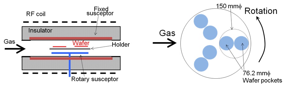
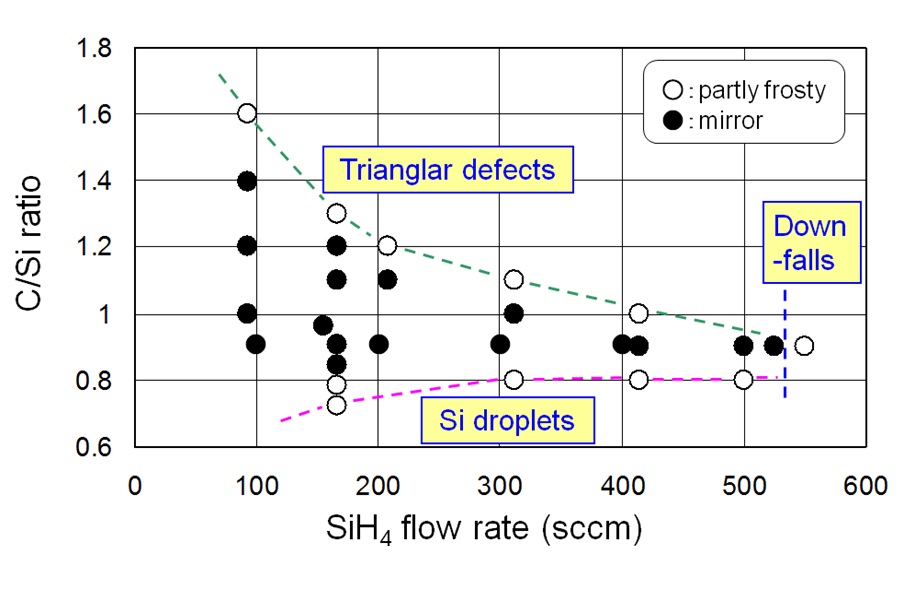
Thick silicon carbide (SiC) epitaxial layers with low background doping are required for high-voltage devices to reduce the maximum electric fields at large reverse biases. SiC {0001} is a polar face, being either silicon-face (Si-face) or carbon-face (C-face). Currently, the Si-face is widely used in research and production of power devices, since the reproducible production of epitaxial layers having background doping levels less than 1015 cm-3 can be easily realized by using a site-competition technique [1-3]. On the other hand, the C-face of 4H-SiC is considered potentially useful for SiC-MOSFET fabrication, because of the higher inversion channel mobility [4]. Due to the background doping level in the C-face epitaxial layer is higher than Si-face epitaxial layer [2], C-face epitaxial layers are getting less popular when used in higher-voltage application. Accordingly, there has been almost no report on the higher growth rate study by using C-face substrate. In our current investigation, reduction in background doping level on C-face epitaxial layers was targeted by increasing the growth rate of 4H-SiC film using a multiple-wafer (3x 150 mm-diameter) epitaxy system with a horizontal low-pressure hot-wall reactor [5]. Precursor gases used were monosilane and propane in hydrogen atmosphere. Growth pressure and temperature were kept 6.3 kPa and 1725 oC, respectively. The substrate used was n-type (000-1) 4H-SiC 4o off-cut toward <11-20>. Two 76.5 mm-diameter wafers were aligned in a 150 mm-diameter pocket to cover radial direction of a rotating susceptor wafer plate holder. Figure 1 shows the experimental set-up. Specular surface was maintained up until the growth rate was 50.9 μm/h when the input C/Si ratio was 0.9. Even when the growth rate was lower than this, outermost position of the wafer became partly frosty in case of making the input C/Si ratio too high or too low. Higher C/Si ratio was found likely to form triangular morphology to retard mirror like surface. Lower than 0.8 in C/Si ratio was found likely to generate silicon droplet also retarding smooth surface growth. The highest growth rate in our system was found limited by morphology deterioration with large density of downfalls. These results were summarized in fig. 2. The uniformity of the film thickness was measured by FTIR and found 2.42% of sigma/mean value on the wafers with the growth rate was 50.9 μm/h. The doping control was found possible with the background level of as low as 4x1014 cm-3 by assuming that residual nitrogen in the atmosphere plays an important role and by reducing it with employing high vacuum process prior to the start of epitaxial growth recipe. Since the formation of in-grown 8H Schokley stacking faults was reported when the SiC epitaxial growth rate was higher [6], photoluminescence imaging was examined with and without the band-pass filter and found that the density of such stacking faults was as low as 0.24cm-2. In addition, surface morphological defects were evaluated using confocal differential interference microscope and the triangular defects were counted. It was found that the defect density becomes larger by increasing the growth rate. However up until the growth rate was within 43.1 μm/h, the triangular defect density was less than 0.32 cm-2. In summary, epitaxial growth on 4H-SiC C-face substrates with the size corresponding to 150 mm was carried out. As high as 50.9 μm/h was achieved as the growth rate without appearing frosty part on the wafers. High uniformity in the film thickness and low doping level control were satisfied at the same time. Also, there has not been found significant density of defects such as in-grown 8H Schockley stacking faults and surface morphological triangular defects within the range of 43.1 μm/h growth rate.
Fig. 1 Experimental set-up used in the present study.
Fig. 2 Surface morphology variation by changing monosilane flow rate and C/Si ratio Acknowledgements: This work is supported by Novel Semiconductor Power Electronics Project Realizing Low Carbon Emission Society under Ministry of Economy, Trading Industry (METI) and New Energy and Industrial Technology Development Organization (NEDO). References: [1] H. S. Kong, J. T. Glass and R. F. Davis, J. Appl. Phys. 64 (1988) 2672. [2] T. Kimoto, A. Itoh and H. Matsunami, Phys. Stat. Solidi (b) 202 (1977) 247. [3] D. J. Larkin, P. G. Neudeck, J. A. Powell and L. G.. Matus, Appl. Phys. Lett. 65 (1994) 1659. [4] K. Fukuda, M. Kato, J. Senzaki, K. Kojima and T. Suzuki, Mat. Sci. Forum 457-460 (2004) 1417. [5] C. Kudou, K. Tamura, T.Aigo, W. Ito, J. Nishio, K. Kojima and T. Ohno, Mat. Res. Soc. Symp. Proc. Vol.1433 (2012) H1.2. [6] S. Izumi, H. Tsuchida, I. Kamata and T. Tawara, Appl. Phys. Lett. 86 (2005) 202108. |
| Legal notice |
|
| Related papers |
Presentation: Oral at 17th International Conference on Crystal Growth and Epitaxy - ICCGE-17, Topical Session 3, by Johji NishioSee On-line Journal of 17th International Conference on Crystal Growth and Epitaxy - ICCGE-17 Submitted: 2013-03-08 10:40 Revised: 2013-03-25 09:37 |