| Search for content and authors |
Suppression of step bunching generated on 4H-SiC Si-face substrates with vicinal off-angle |
| Keiko Masumoto 1,2, Kentaro Tamura 1,3, Sachiko Ito 1,2, Kazutoshi Kojima 1,2, Hajime Okumura 1,2 |
|
1. R D Partnership for Future Power Electronics Technology (FUPET), Onogawa 16-1, Tsukuba 305-8569, Japan |
| Abstract |
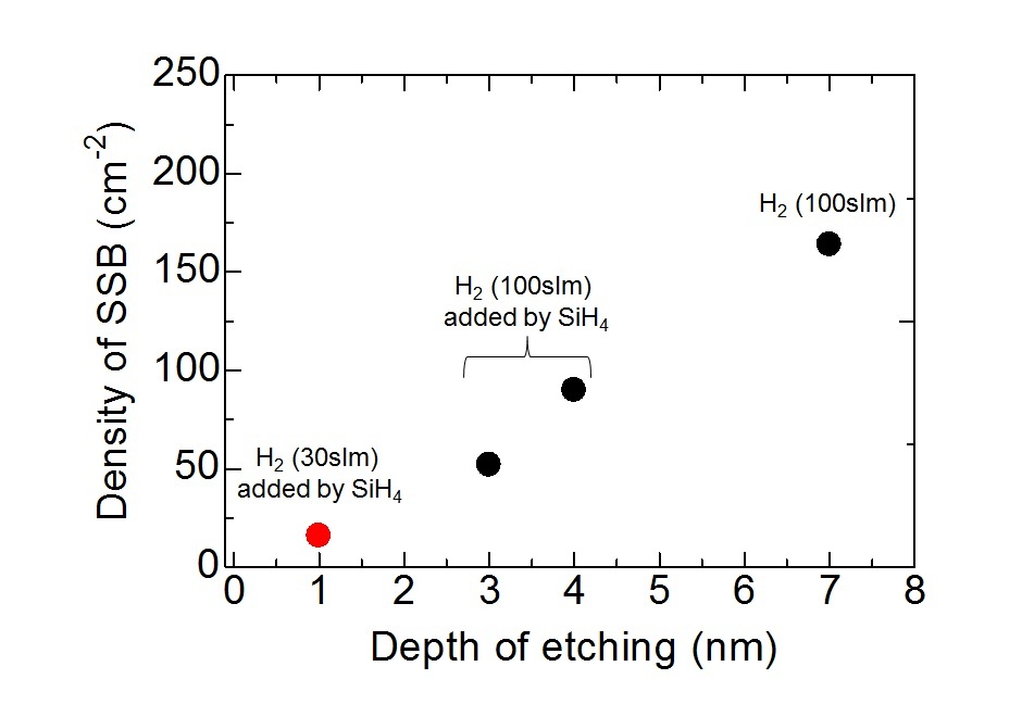
SiC homoepitaxial layers grown on substrates with vicinal off-angle (epi-layers with vicinal off-angle) are effective for suppressing anisotropy of SiC trench devices. Step bunching, however, is easily generated on the substrates with vicinal off-angle during increase in temperature at H2 atmosphere prior to the growth of the epi-layers. It is indispensable to suppress the generation of step bunching during increase in temperature in order to improve the surface morphology of the epi-layers with vicinal off-angle. It is thought that the etching reactions between the surface of the substrates and H2 gas should be suppressed in order to suppress the generation of step bunching. In this study, we have investigated the process for suppressing the etching reactions during increase in temperature prior to the growth of the epi-layers. We used the 4H-SiC Si-face substrates with vicinal off-angle (0.9 deg.). The etching process was conducted in a horizontal hot-wall CVD reactor at a temperature of 1660 °C and a pressure of 10.3 kPa for 1 min. It has been reported that the etching rate is lowered by adding a source gas such as SiH4 and C3H8 and by reducing the flow rate of H2 [1,2]. Therefore, we investigated the effects of adding SiH4 and C3H8 and of reducing the flow rate of H2 on the etching depth and the generation of step bunching. Firstly, we observed a substrate etched by using H2 of 100 slm. The etching depth was estimated at 7 nm. It has been reported that basal plane dislocations generate giant step bunching with finite length which is called short step bunching (SSB) [3]. We found that SSB, whose height and length was over 5 nm and about 1 mm, respectively, was generated on the substrate. The density of SSB generated on the substrate was about 200 cm-2. Secondly, we investigated substrates etched by adding each of SiH4 and C3H8. The etching depth of the substrate was decreased to 3-4 nm by adding each of SiH4 and C3H8. The density of SSB was not reduced by adding C3H8 but reduced by adding SiH4. It is thought that both the reduction of the etching depth and the etching in an Si-rich environment are important for suppressing the generation of SSB. Finally, we tried to suppress the etching reactions by reducing the flow rate of H2 added by SiH4. The etching depth was decreased to 1 nm by reducing the flow rate of H2 to 30 slm. As a result, the density of SSB was decreased to 16 cm-2 as shown in the Figure. We have found that the etching reactions between the SiC substrates with vicinal off-angle and H2 gas were suppressed by adding SiH4 and reducing the flow rate of H2 at once. As a result, we have succeeded in drastically decreasing the density of SSB. We will present the detail of the differences between the addition of SiH4 and that of C3H8, and the growth of epitaxial layers using this process at the conference. Acknowledgement This work is supported by Novel Semiconductor Power Electronics Project Realizing Low Carbon Emission Society under New Energy and Industrial Technology Development Organization (NEDO). References [1] K. Kojima et.al., Mater. Sci. Forum 556-557 (2007) 85. [2] J. Zhang et.al., Mater. Sci. Forum 389-393 (2002) 239. [3] K. Tamura et.al., Ext. Abstr. 21st Meeting on SiC and Related Wide Bandgap Semiconductors (2012) 6 [in Japanese].
|
| Legal notice |
|
| Related papers |
Presentation: Oral at 17th International Conference on Crystal Growth and Epitaxy - ICCGE-17, Topical Session 3, by Keiko MasumotoSee On-line Journal of 17th International Conference on Crystal Growth and Epitaxy - ICCGE-17 Submitted: 2013-03-25 09:12 Revised: 2013-03-25 09:34 |