| Search for content and authors |
Epitaxial growth on porous substrates of III-V semiconductors |
| Jan Grym 1, Peter Gladkov 1, Jan Vaniš 1, George P. Dimitrakopulos 2, Calliope Bazioti 2, Philomela Komninou 2, Eduard Hulicius 3, Jiří Pangrác 3, Oliva Pacherová 3 |
|
1. Czech Academy of Sciences, Institute of Photonics and Electronics, Chaberská 57, Prague 18251, Czech Republic |
| Abstract |
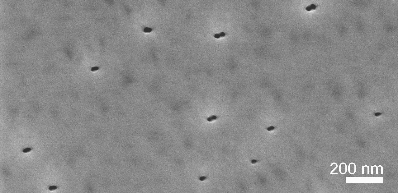
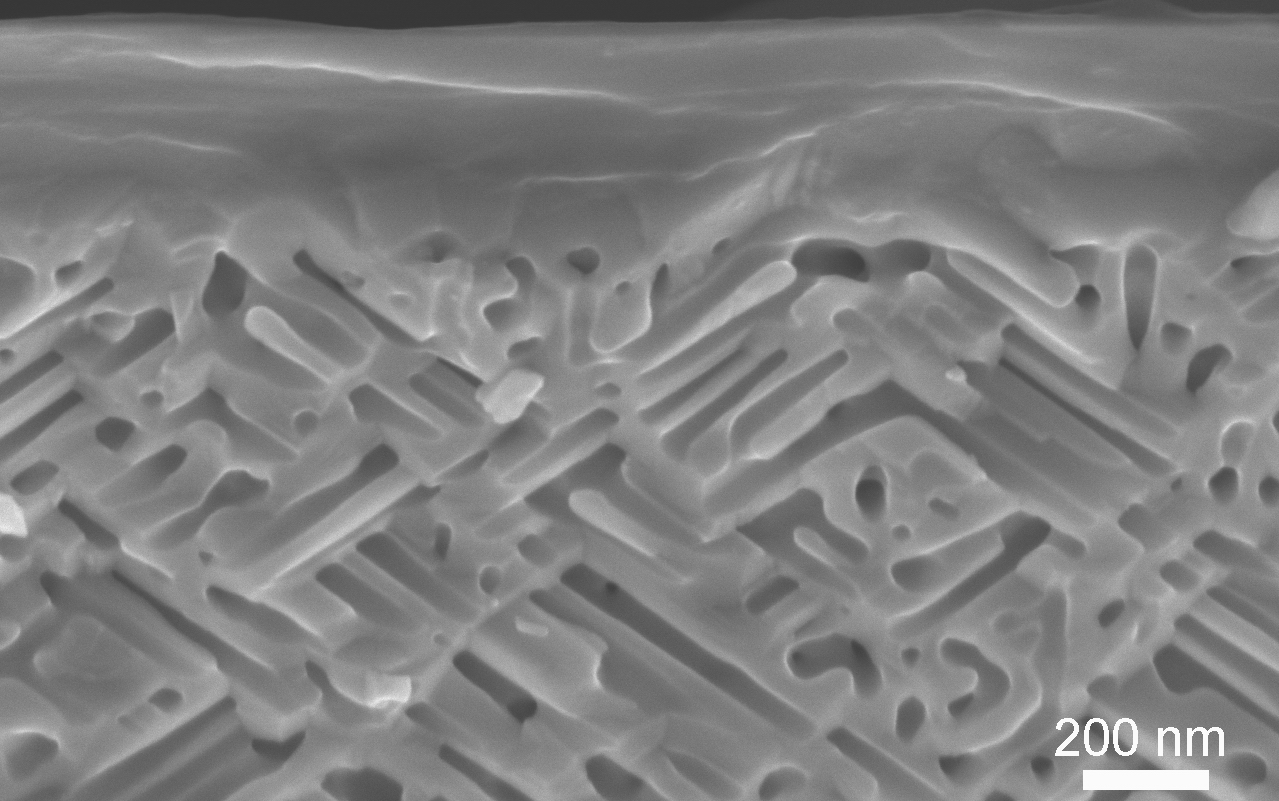
In mismatched heteroepitaxial growth on a conventional substrate, a thin epitaxial layer accommodates all of the mismatch strain so that this layer must be kept below the critical layer thickness to avoid generation of misfit dislocations, which are detrimental for the performance, reliability and lifetime of semiconductor devices. Enhancement of the critical layer thickness would be beneficial in many applications. One of the unexplored approaches to achieve the enhancement consists in the growth on a porous substrate, which, thanks to its compliance, is supposed to be capable of accommodating elastic strains at the heteroepitaxial interface. We report on the electrochemical preparation of porous substrates of InP and GaAs and discuss specific problems related to their application in epitaxial growth from the liquid and vapor phase. The pore etching was carried out in an electrochemical cell using a three-electrode configuration. A home-made potentiostat/galvanostat was computer-controlled and allowed to register all process variables. The porous substrates and epitaxial layers were prepared by liquid phase epitaxy (LPE) and metal-organic vapor phase epitaxy (MOVPE) were characterized by scanning electron microscopy (SEM), focused ion beam microscopy (FIBM), cross sectional transmission electron microscopy (XTEM), atomic force microscopy (AFM), x-ray diffraction (XRD), and low temperature photoluminescence spectroscopy (PL). Porous substrates with low surface roughness and low density of pores in the nucleation layer (on the substrate surface) are appreciated to be easily laterally overgrown at an early stage of epitaxy; the pores should branch below this nucleation layer and thus allow for a high porosity and uniformity of a porous layer. This was achieved in highly concentrated HCl for InP substrates and HF-KI based electrolyte for GaAs substrates. A set of samples of InGaAs/GaAs MOVPE experiments with a different composition of the ternary alloy (5, 10 and 20 % of In) and different thickness of the layer below and above the expected critical value on both porous and monolithic substrates was intentionally prepared for XRD and TEM measurements. Significantly higher amount of elastic strain was retained in the layers deposited on porous substrates and the density of misfit dislocations was reduced as compared to the layers grown on conventional substrates in the same growth run. Several systems on porous substrates were also grown by LPE. Direct LPE deposition of InAs on conventional InP substrates (lattice mismatch approximately 3.4%) resulted in extremely poor structural quality polycrystalline deposit. On a porous InP substrate, epitaxially textured monocrystalline grains of InAs were obtained. Stress at the interface was proved to have a large impact on the mass transport velocity within the porous layer at elevated temperatures. A large set of InGaAs layers grown on porous GaAs was prepared at 590 C. Layers on porous substrates were systematically thicker, had higher integral luminescence intensity and allowed to introduce larger amount of indium. Growth conditions for the preparation of smooth layers with a good surface morphology were established.  SEM picture of the surface of the low-roughness porous GaAs substrate 
SEM picture of the cross-section of the low-roughness porous GaAs substrate 
SEM picture of the cross-section of the InGaAs layer with 20 % of In grown by MOVPE on porous GaAs substrate Work supported under the 2011-2013 Greece-Czech bilateral R&D collaboration project “III-V semiconductor heterostructures/nanostructures towards innovative electronic and photonic applications”. |
| Legal notice |
|
| Related papers |
Presentation: Poster at 17th International Conference on Crystal Growth and Epitaxy - ICCGE-17, General Session 10, by Jan GrymSee On-line Journal of 17th International Conference on Crystal Growth and Epitaxy - ICCGE-17 Submitted: 2013-04-12 17:20 Revised: 2013-05-18 00:44 |