| Search for content and authors |
Growth and characterization of AlxGa1-xN/GaN/ Al2O3 heterostuctures |
| Arivazhagan Ponnusamy , Ramesh Raju , Jayasakthi Mathaiyan , Loganathan Ravi , Prabakaran Kandhasamy , Balaji Manavaimaran , Baskar Krishnan |
|
Crystal Growth Centre, Anna University, Chennai, Chennai 600025, India |
| Abstract |
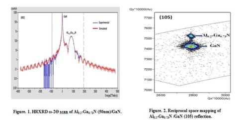
The strain free AlxGa1-xN(x= 0.23) and partially strained AlxGa1-xN(x= 0.27) have been grown on GaN/sapphire template using MOCVD. The composition of Al in AlGaN layer has been determined from the ω-2Θ scan. Figure.1 shows the ω-2Θ scan for Al0.27Ga0.73N /GaN layer. The Reciprocal space mapping (RSM) of (105) reflection has been carried out for AlxGa1-xN(x= 0.23 and 0.27)/GaN layers and the in-plane strain of the AlxGa1-xN epilayers with respect to GaN has been estimated. Figure.2 illustrates the RSM of (105) reflection for Al0.27Ga0.73N /GaN layer. Figure .3 shows the band edge emissions at 320 nm and 312 nm corresponding for Al0.23Ga0.77N and Al0.27Ga0.73N respectively, whereas the 362 nm emission is for GaN. The root mean square (RMS) surface roughness of Al0.23Ga0.77N and Al0.27Ga0.73N has been estimated as 0.37 nm and 0.30 nm respectively using atomic force microscopy. Ti/Al/Ni/Au: 200/1000/400/500 Å metal layers were deposited onAlxGa1-xN(x= 0.23) and AlxGa1-xN(x= 0.27) layers by E-beam evaporation technique. The samples were annealed with two step annealing in rapid thermal annealing system at optimum conditions of 550 ˚C under N2 ambient for 60 s and at 780 ˚C for 30 s. 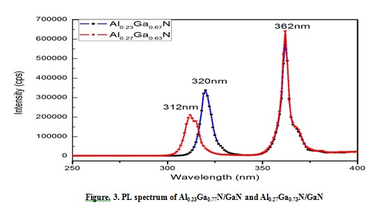 The Circular Transmission Line Measurement (CTLM) has been adopted to find the variation in contact resistance (Rc), transfer length (LT)and specific contact resistance(ρc) between metal contacts (Ti/Al/Ni/Au: 200/1000/400/500 Å) and AlxGa1-xN layers were determined using I-V characteristics of diodes. The Circular Transmission Line Measurement (CTLM) has been adopted to find the variation in contact resistance (Rc), transfer length (LT)and specific contact resistance(ρc) between metal contacts (Ti/Al/Ni/Au: 200/1000/400/500 Å) and AlxGa1-xN layers were determined using I-V characteristics of diodes.
In addition the schottky behavior of Ni/Au: 400/1500 Å contacts on the strain free AlxGa1-xN(x= 0.23) and partially strained AlxGa1-xN(x= 0.27) layers have been studied using current -voltage (I-V) and capacitance-voltage(C-V) measurements. The device characteristics have been correlated with the structural quality of AlxGa1-xN layers.
REFERNCES: [1] P. Gay, P. B. Hirsch and A. Kelly, Acta Metall. 1, 315 (1953). [2] C. G. Dunn and E. F. Koch, Acta Metall. 5, 548 (1957). [3] G. S. Huang, T. C. Lu, H. H. Yao, H. C. Kuo, and S. C. Wang, Appl. Phys. Lett. 88, 061904, (2006). [4] B. Jacobs, M.C.J.C.M. Kramer , E.J. Geluk, F. Karouta, Journal ofCrystal Growth, Vol. 241, pp. 15, 2002. [5] L.F. Lester, J.M. Brown, J.C. Ramer, L. Zhang, S. D. Hersee, J.C. Zolper, Applied Physics Letters, Vol. 69,No. l8,p. 2737, 1996. |
| Legal notice |
|
| Related papers |
Presentation: Poster at 17th International Conference on Crystal Growth and Epitaxy - ICCGE-17, Topical Session 3, by Baskar KrishnanSee On-line Journal of 17th International Conference on Crystal Growth and Epitaxy - ICCGE-17 Submitted: 2013-04-15 15:02 Revised: 2013-07-18 12:01 |