| Search for content and authors |
Structural and optical characterization of AlGaN/GaN layers |
| Jayasakthi Mathaiyan , Ramesh Raju , Arivazhagan Ponnusamy , Loganathan Ravi , Prabakaran Kandhasamy , Balaji Manavaimaran , Baskar Krishnan |
|
Crystal Growth Centre, Anna University, chennai 600025, India |
| Abstract |
Group III-nitride semiconductors of wurtzite structure are of great scientific and technological interest due to their potential application in short-wavelength light-emitting devices such as light-emitting diodes (LEDs) and laser diodes (LDs), in high temperature and high power electronic devices [1]. Aluminum rich AlxGa1-xN alloys are promising materials for deep ultraviolet light emitting diodes (DUV-LEDs). DUV LEDs hold enormous potential for many applications such as sterilization, water purification and chemical agent detection [2]. AlxGa1-xN/GaN epilayers were grown on c-plane sapphire substrate by Metal-Organic Chemical Vapor Deposition (MOCVD). The reagents were 7N pure ammonia (NH3), trimethylgallium (TMGa) and trimethylaluminum (TMAl). Hydrogen and nitrogen purified by purifier were used as carrier gas. During the growth TMAl flow was varied whereas the reactor pressure, NH3 flow, reactor temperature, TMGa flow were kept constant. 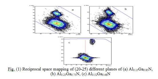
The crystalline quality of the samples was determined by high resolution X-ray diffraction (HRXRD) rocking curve of symmetric (0004) and asymmetric reflection (10-12) for GaN and AlGaN. The thickness of the AlGaN was determined from (0004) ω/2θ-scan. HRXRD reciprocal space mapping (RSM) of (20-25) axis is used to estimate the strain in the AlGaN/GaN layers as shown in fig (1). The estimated degree of lattice relaxation of 2.29 x 10⁻⁴ for Al0.15Ga0.85N, indicates that the AlGaN epilayers is fully strained and pseudomorphic to the underlying GaN layer. RSM results indicate that in low Al composition AlGaN and GaN layers are fully strained and no cracks were observed in SEM. In high Al composition (> 0.33) strain relaxation between AlGaN and GaN epilayers resulted in cracks on the surface of the samples. Also the growth rate of AlGaN decreases on increasing the aluminum composition in fig (2). 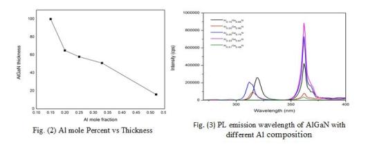
The optical properties were studied by room temperature PL. The GaN emission wavelength of 362 nm and the AlGaN emission wavelengths in the region 324-287 nm were estimated for different Al composition fig (3). The surface morphology and cracks in AlGaN epilayers were studied by Scanning Electron Microscopy (SEM). The surface roughness of AlGaN epilayers was studied by Atomic Force Microscopy (AFM). The surface roughness was found to be increased in AlGaN layers and strain relaxation between AlGaN and GaN were observed in higher aluminum composition. Higher in-plane tensile strain due to lattice and thermal mismatch between high Al content AlGaN layers and GaN buffer might be attributed to the formation of cracks. An increase in flow rate of TMAl, decreased the growth rate and thickness. Efforts are being made to introduce strained layer super lattices and thick AlN buffer layers to grow high quality crack free high aluminum containing layers of AlGaN for UV applications and results will be discussed. References
|
| Legal notice |
|
| Related papers |
Presentation: Oral at 17th International Conference on Crystal Growth and Epitaxy - ICCGE-17, General Session 10, by Baskar KrishnanSee On-line Journal of 17th International Conference on Crystal Growth and Epitaxy - ICCGE-17 Submitted: 2013-04-15 13:09 Revised: 2013-05-27 19:15 |