| Search for content and authors |
Studies on dislocation and surface morphology of AlxGa1-xN/GaN heterostructures grown by MOCVD |
| Loganathan Ravi , Jayasakthi Mathaiyan , Ramesh Raju , Arivazhagan Ponnusamy , Prabakaran Kandhasamy , Balaji Manavaimaran , Baskar Krishnan |
|
Crystal Growth Centre, Anna University, Chennai, Chennai 600025, India |
| Abstract |
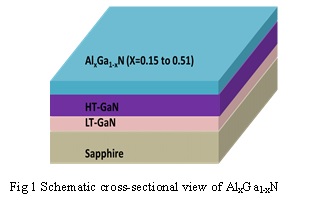
| Group III-nitride semiconductors have attracted huge research interest due to its unique properties and potential application for short-wavelength light emitters, high temperature and high frequency devices [1]. Successful fabrication of III-nitride based devices depends on the ability to grow epitaxial films on sapphire with low defect density. The large lattice mismatch and thermal expansion coefficient mismatch between AlGaN/GaN and sapphire substrate generally cause high-density of threading dislocations (TDs). TDs are very harmful to electronic and photonic devices [2]. GaN epilayer on sapphire typically contains the high-density of dislocations in the order of 108 to 1010 cm-2
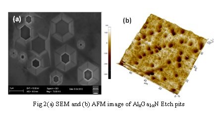
. Therefore, it is of great interest to explore a reliable and quick method for investigating dislocations in AlGaN/GaN heterostructures. To characterize the dislocation density of AlGaN/GaN heterostructures, various evaluation techniques such as high resolution X-ray diffraction (HRXRD), cathodoluminescence (CL), photoluminescence (PL), atomic force microscopy (AFM), and transmission electron microscopy (TEM) have been adopted [3]. In the present study, the AlxGa1-xN epilayers with 0 ≤ x ≤ 0.51 on GaN layers were grown by Metal Organic Chemical Vapour Deposition (MOCVD) method. Fig (1) shows typical cross-sectional view of AlxGa1-xN /GaN heterostructures on sapphire substrate. The dislocation density of the samples has been estimated through wet-chemical etching and HRXRD. The FWHM of (002) plane of GaN layers, estimated from ω-scan was in the range of 342-404 arc-sec, whereas FWHM of (102) plane was in the range 632-999 arc-sec. Ortho phosphoric acid (H3PO4) has been used as chemical etchant for AlGaN/GaN samples. The wet etching process has been optimized by varying the etching time and temperature. H3PO4 at 180 ºC for 90 seconds has been found as the optimal etching condition for AlGaN/GaN samples. After etching, the AlGaN/GaN samples have been analysed by SEM and AFM. Figure 2(a) shows the SEM image of etch pits and figure 2( b) shows the AFM image of etch pits formed on the surface of AlGaN layers. The dislocation density of the samples was found to be between 2.1x108cm-2 and 1.9x109cm-2. Photoluminescence studies reveal that the near band edge (NBE) emission intensity of AlGaN and GaN layers increases after etching due to increases the surface roughness. The dislocation density estimated from etch pits has been correlated with HRXRD results. References [1] Yitao Liao, Christos Thomidis, Chen-kai Kao, and Theodore D. Moustakas, “AlGaN based deep ultraviolet light emitting diodes with high internal quantum efficiency grown by molecular beam epitaxy” Appl. Phys. Lett., Vol. 98, pp. 081110, 2011. [2] D. Kapolnek, X. H. Wu, B. Heying, S. Keller, B. P. Keller, U. K. Mishra, S. P. DenBaars, and J. S. Specka, “Structural evolution in epitaxial metalorganic chemical vapor deposition grown GaN films on sapphire” Appl. Phys. Lett., Vol. 67, pp. 1541-1543, 1995. [3] J.L. Weyher, S. Lazar, L. Macht, Z. Liliental-Weber, R.J. Molnar, S. Mu¨ ller,V.G.M. Sivel, G. Nowak and I. Grzegory “Orthodox etching of HVPE-grown GaN” Journal of Crystal Growth, Vol. 305,pp. 384–392, 2007. |
| Legal notice |
|
| Related papers |
Presentation: Poster at 17th International Conference on Crystal Growth and Epitaxy - ICCGE-17, Topical Session 3, by Baskar KrishnanSee On-line Journal of 17th International Conference on Crystal Growth and Epitaxy - ICCGE-17 Submitted: 2013-04-15 12:12 Revised: 2013-07-18 11:49 |