| Search for content and authors |
Creations of vacancy on growth interface during silicon melt growth by decreasing pulling rate |
| Takao Abe 1, Toru Takahashi 1, Koun Shirai 2 |
|
1. Shin-Etsu Handotai Co., Ltd. (SEH), Isobe RD Center 2-13-1 Isobe, Annaka 379-0196, Japan |
| Abstract |
| 1. Introduction
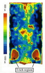
Almost people in the field of point defects research in silicon crystals have believed that both point defects coexist in growth interface. However, our following experimental results show that the growth interface is always filled with vacancies. On the other hand, interstitials are created far from the growth interface when and where the thermal gradient is increased. 2. Experiments Since a 100 mm CZ crystal grown with 1.4 mm/min pulling rate was reached at stationary state, it was grown with gradually decreased pulling rate until 0.5 mm/min and finally it was detached from the melt and rapidly cooled. The crystal was cut parallel to growth direction with 1.0 mm in thickness and then annealed at 1000 oC, 16 hrs in dry O2. Figure 1 is an x-ray topograph of the specimen. The black contrast shows the strong x-ray diffraction intensity from oxygen precipitates (SiO2). Such oxygen precipitation induced by one step annealing is called as the AOP (anomalous oxygen precipitation) [1] which presents that the existence of isolated vacancies before aggregation to produce a COP (crystal originated particle) [2] = void [3]. On the other hand, the existence of I is confirmed by using a WLT (wafer lifetime) method. Since the minority carriers induced by light are trapped by silicon dangling bonds which interstitial type dislocation loops have, the lifetime value is decreased. In both side regions under part of Fig. 2 the decreased WLT region is confirmed. In Fig. 1 the three traces of growth interface shapes which are actually marked in the crystal by decreasing of crystal rotation rate for 30 second are seen. One is strong concave interface to a melt at 1.4 mm/min when decreasing pulling rate starts, second is weak concave shape at 1.0 mm/min and third is flat shape at 0.6 mm/min. 3. Results In Fig. 1 the black contrast part like a wine glass shape is the V rich region which is formed by the AOP annealing. The upper white contrast part is the COP region which is produced by the aggregation of individual V. The lower both sides white regions are confirmed as I rich regions by the WLT map as seen in Fig. 2.
Fig. 2 WLT map of as grown crystal of Fig. 1. Finally it is confirmed that the growth interface and neighbor grown region with the denser black color shows the high density V region. According to the traditional Voronkov model [4], the growth interface should be the interstitial rich region with 0.6 mm/min pulling rate. However, even the growth interface with 0.5 mm/min pulling rate, the growth interface is filled with vacancy. 4. Conclusion From the above results it is concluded that the growth interface is always filled with vacancy but interstitial is not existed. Interstitials are created far from the growth interface induced by a large thermal gradient.References [1] H. Harada, T. Abe, J. Chikawa, in: H.R. Huff, T. Abe, B.O. Kolbesen (Eds.) Semiconductor Silicon 1986, the Electrochem. Soc., Pennington, NJ, 1986, p. 76. [2] J. Ryuta, E. Morita, T. Tanaka, Y. Shimanuki, Jpn. J. Appl. Phys. 29 (1991) L1947 [3] M. Itsumi, H. Akiya, T. Ueki, M. Yamawaki, J. Appl. Phys. 78 (1995) 5984. [4] V.V. Voronkov, J. Cryst. Growth 59 (1982) 625. |
| Legal notice |
|
| Related papers |
Presentation: Oral at 17th International Conference on Crystal Growth and Epitaxy - ICCGE-17, General Session 1, by Takao AbeSee On-line Journal of 17th International Conference on Crystal Growth and Epitaxy - ICCGE-17 Submitted: 2013-04-12 08:46 Revised: 2013-07-18 23:07 |
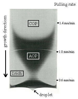 Fig. 1 X-ray topograph after AOP annealing of CZ crystal grown gradually decreased pulling rate and finally detached from melt.