| Search for content and authors |
Creations of interstitial inside crystal during silicon melt growth by heating melt |
| Takao Abe 1, Toru Takahashi 1, Koun Shirai 2 |
|
1. Shin-Etsu Handotai Co., Ltd. (SEH), Isobe RD Center 2-13-1 Isobe, Annaka 379-0196, Japan |
| Abstract |
| 1. Introduction
Almost researchers in the field of point defects in silicon crystals have believed that both point defects coexist in growth interface. However, our following experimental results show that the growth interface is always filled with vacancy (V). On the other hand, interstitial (I) is created at a region to be long way from the growth interface, depending on increasing thermal gradient. 2. Experiments Three 100 mm CZ crystals with 1.4 mm/min pulling rate were grown from the same melt in one crucible and then they were detached from the melt during growth and cooled rapidly. They were cut parallel to growth direction to obtain specimens with 1.0 mm in thickness and were annealed with 1000℃, 16hrs in dry O2. Their x-ray topographs were obtained as seen in Fig. 1, 2 and 3. Where the black contrast shows the strong intensity of x-ray diffraction from oxygen precipitates (SiO2). Such oxygen precipitation induced by only one step annealing is called as the AOP (anomalous oxygen precipitation) [1], which presents that the existence of isolated vacancies before producing a COP (crystal originated particle) [2] = void [3] by aggregation. 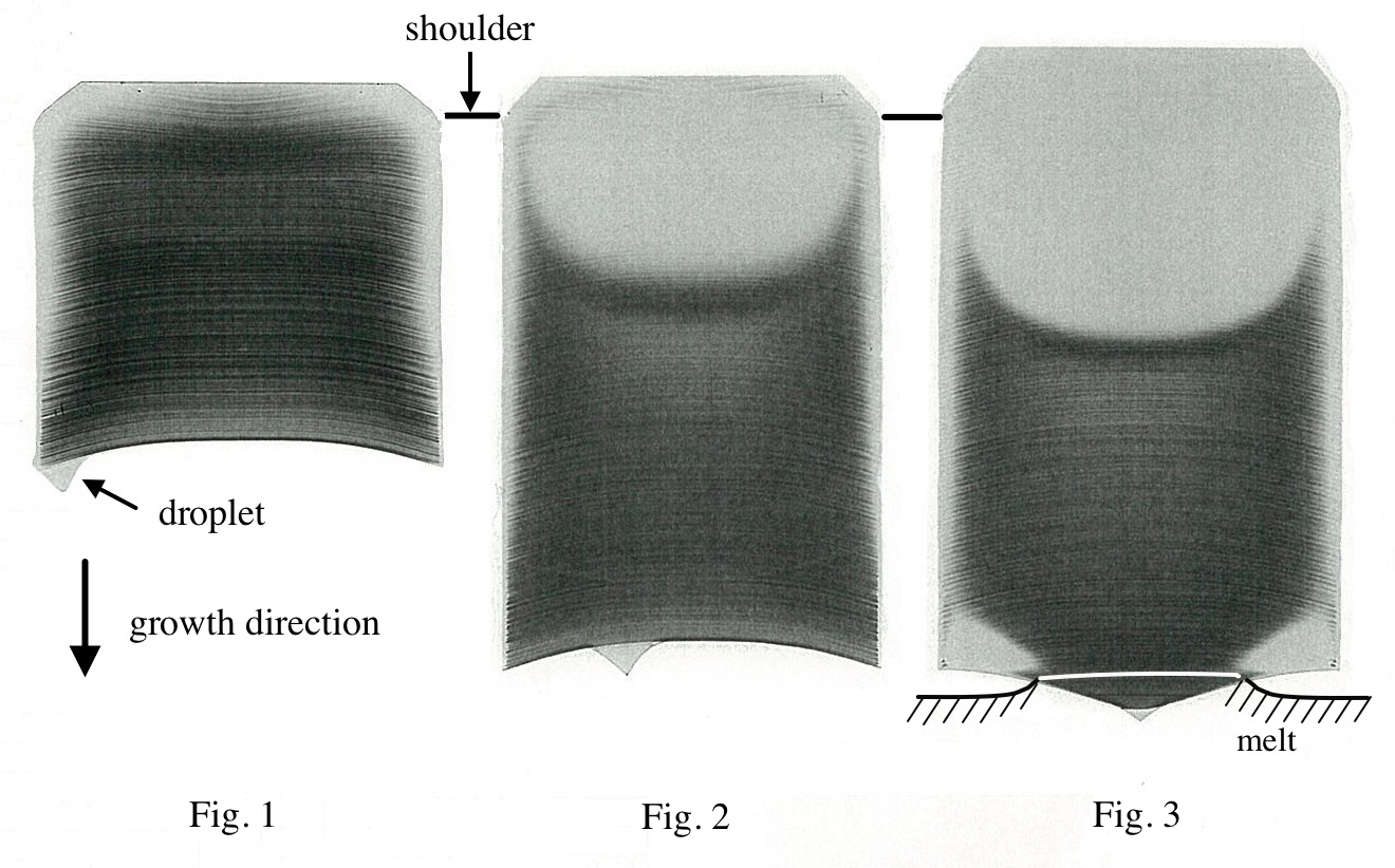
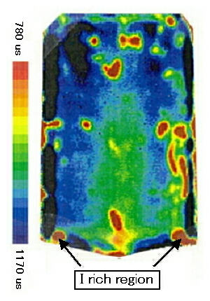
Fig. 1 and 2 X-ray topographs after AOP annealing of mechanically detached CZ crystals at 50 mm from shoulder position and at 100 mm, respectively. Fig. 3 X-ray topograph after AOP annealing of partially detached CZ crystal by heating melt for 30 min and finally detached it mechanically. Schematic drawings of interface shape and meniscus of melt. On the other hand, the existence of I is confirmed by using a WLT (wafer lifetime) method. Since the minority carriers induced by light are trapped by silicon dangling bonds of interstitial type dislocation loops, the lifetime value is decreased with increasing the density of the dislocation loop. In both side regions under part of Fig. 3, the decreased WLT region is confirmed. 3. Results and discussions The first crystal as shown in Fig. 1 was detached from the melt at length of 100 mm from crystal shoulder. It is understood from the AOP distribution that almost whole crystal except surface area of the shoulder is V rich. The second crystal as shown in Fig. 2 was grown 50 mm in length and 36 min in period longer than those of the first crystal and was detached and cooled. During longer growth period the COP region is newly generated and spread 40 mm in depth from the shoulder level. This means that individual V in the AOP region aggregates to make a void. When the third crystal as seen in Fig. 3 was grown at the same length (150 mm) with the second crystal, instead of the mechanical detaching procedure the melt temperature was continuously increased for 30 min by increasing the input power. As the result both sides of peripheral area of the growth interface was separated from the melt but in the center area was grown continuously due to large cooling effect by pulling stop. The above explanations are recognized using a schematic line drawn along growth striations in Fig. 3. That is, the growth interface is deeply concave to the melt just at pulling stop but after that the interface shape becomes gradually deeply convex in center area. Finally the crystal was mechanically detached after 30 min from pulling stop. It is clear that the area where crystal contacts with the melt is always V rich but the both sides peripheral area where crystal does not contact with the melt are replaced by I rich region. The white contrast area in x-ray topograph in Fig. 3 corresponds to the low lifetime area where is the I rich region in WLT map in Fig. 4.
Fig. 4 WLT map of as grown crystal of Fig. 3 If the crystals which do not contact with the melt are heated up, the I is created. This fact was already reported by Roksnoer [4]. However, it is observed in our growing experiments that the V rich region converts into the I rich region in one crystal during growth. The third crystal was grown 30 min longer period than that of the second crystal so that the depth of the COP region elongated to 60 mm. It is recognized that in standard crystal growth procedure the whole crystal becomes the COP crystal due to gradually cooling without detaching. 4. Conclusion From the above results it is concluded that the growth interface is always filled with vacancy but interstitial is not existed. Interstitials are created far from the growth interface induced by a large thermal gradient. References [1] H. Harada, T. Abe, J. Chikawa, in: H.R. Huff, T. Abe, B.O. Kolbesen (Eds.) Semiconductor Silicon 1986, the Electrochem. Soc., Pennington, NJ, 1986, p. 76. [2] J. Ryuta, E. Morita, T. Tanaka, Y. Shimanuki, Jpn. J. Appl. Phys. 29 (1991) L1947 [3] M. Itsumi, H. Akiya, T. Ueki, M. Yamawaki, J. Appl. Phys. 78 (1995) 5984. [4] P.J. Roksnoer, J. Cryst. Growth 68 (1984) 596. |
| Legal notice |
|
| Related papers |
Presentation: Poster at 17th International Conference on Crystal Growth and Epitaxy - ICCGE-17, General Session 1, by Takao AbeSee On-line Journal of 17th International Conference on Crystal Growth and Epitaxy - ICCGE-17 Submitted: 2013-04-12 06:17 Revised: 2013-07-16 12:57 |