| Search for content and authors |
Discrepancies between experimental results and simulations on point defects behavior during silicon crystal growth from the melt |
| Takao Abe 1, Toru Takahashi 1, Koun Shirai 2 |
|
1. Shin-Etsu Handotai Co., Ltd. (SEH), Isobe RD Center 2-13-1 Isobe, Annaka 379-0196, Japan |
| Abstract |
1. Introduction In order to confirm justification for Voronkov’s model, analyses were done by the detailed comparison between our experimental secondary defect distributions in CZ crystal and the simulation results on point defects distribution by Dornberger et al., who had explained our experimental distribution. The experimental secondary defect distributions were obtained from the defects formed in as grown crystal when the pulling rate is abruptly changed at a time. The simulation is based on Voronkov’s model which gives the boundary between both interstitial and vacancy rich regions to be defined by the sign of CI-CV , where CI and CV are the concentrations of interstitial and vacancy, respectively. They have been performed the simulation for our transient growing process. It is shown from the analyses that there are the discrepancies between our experimental and their simulation results. 2. The experiments on decreasing abruptly pulling rate(DAPR) 2.1 Experiments The measurable defects are not point defects but secondary defects which are formed by recombination and coalescence of point defects. Thus, the point defect distribution is always a speculated one from the secondary defect distribution. It is well known that these secondary defects are only voids and dislocation loops to correspond to vacancies and interstitials, respectively. However, the secondary defects are disclosed by many methods as lifetime, etching, and x-ray topograph, in particular, for the etchings it are well known FPD and OCP correspond to the void, and SEPD corresponds to the dislocation loop in CZ crystals. Also, the same says for the etching for FZ crystals When pulling rate was decreased abruptly, the distributions of secondary defects in the crystals were formed by the recombination and the coalescence of point defects. The distribution was obtained from the lifetime map of minority carriers injected by the infrared pulsed light [1,2]. The samples were prepared from the crystals in three different diameters (50 mm, 100 mm and 200 mm). The crystals were grown from the one crucible with the same melt volume to maintain the same growth condition. The growth condition is that pulling rate (v) is 1.0 mm/min after arriving at a stationary growth, and then abruptly decreased 0.2 mm/min at a time and kept for 30 min, and finally returned 1.0 mm/min again. These crystals were cut off wafers with 1.0 mm in thickness which were parallel to growth direction. And the wafers have the centers at abruptly decreased positions. The lifetime maps of minority carriers for their wafers were shown in Fig. 1(a), (b) and (c), respectively. 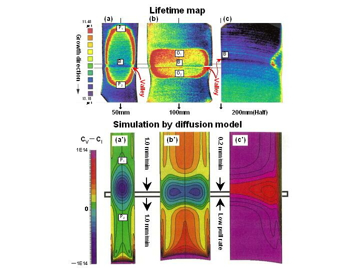
Fig. 1. (a), (b) and (c) show lifetime maps (WT-85 SEMILAB) of as-grown crystals of 50 mm, 100 mm, right half of 200 mm in diameter, respectively. (a’), (b’), (c’) simulation results to correspond with (a), (b) and (c), respectively. 2.2 The interstitial type dislocation loops detected by the minority carrier lifetime The lifetime values are not influenced by the existence of vacancies and their secondary defects so-called FPD (flow pattern defect) [3] or the void [4], but they are adversely proportional to the density of the dangling bonds of dislocations. The interpretation of the lifetime as described above has not yet reported but we show two examples for this interpretation to be true. Figure 2(a) shows an x-ray topograph of a vertical cut wafer along growth direction of an as-grown crystal of which slip dislocations were formed at the growth interface and were spread to the already grown dislocation-free region to relax the thermal stress contained in the CZ crystal grown with a dislocation-free state. Figure 2(b) also shows a lifetime map of the wafer in Fig. 2(a). Although all growth condition of the wafer from top to bottom is the same, the lifetimes largely decreased in the dislocated region, and also the lifetimes along the slip dislocations had lower values than those in the dislocation-free region. Figure 3(a) shows an x-ray topograph after copper decoration of the FZ wafer to have been cut parallel to growth direction. This crystal was grown with the abruptly changed pulling rate from 3.0 mm/min to 2.0 mm/min. The decreasing of pulling rate started from the left hand side. Before the change of pulling rate the all region of the crystal was filled with the FPD which is called the D defect in FZ crystals [5]. However, because of decreasing the pulling rate, the SEPD (Secco etch pit defect) [6] region which is called the A defect region in FZ crystals gradually spread into the insides but saturated soon. As shown in Fig. 3(b) which is the magnification of the part to be surrounded by the white lines in Fig. 3(a), the A defects were the arrays of small points which consist of interstitial type dislocation loops with several tens um in size [7] on the growth striations. On the other hand, the lifetime map of a neighboring as-grown wafer is shown in Fig. 3(c) and the A defect region corresponds clearly to the lower lifetime region. The cause of the lower lifetimes should be attributed to the density of the dangling bonds of the dislocation loops. Hence, it is concluded that the low lifetime distributions in Figs. 1(a), (b) and (c) correspond to the density distributions of the dangling bonds on the interstitial type dislocations which were formed by coalescence of interstitial point defects. This conclusion gives us one of the keys to translate the secondary defect distribution into the speculated distribution of point defects. The other key is the lifetime not to be influenced by the existence of vacancies and their secondary defects, that is, voids. 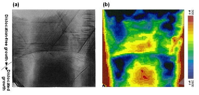
Fig. 2. (a) shows x-ray topograph of dislocated crystal part during (100) CZ growth. (b) Lifetime map (WT-2000 SEMILAB) of wafer (a). 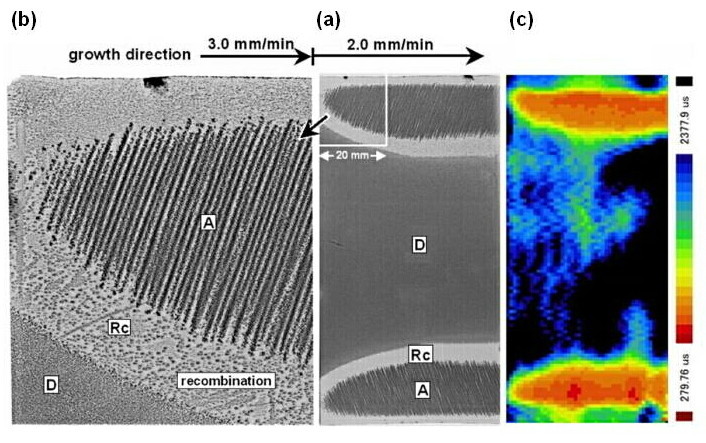 Fig. 3. (a) shows x-ray topograph after copper decoration of wafer cut parallel to growth direction from 100 mm FZ crystal which pulling rate was abruptly changed from 3 mm/min to 2 mm/min. (b) enlargement of upper left square of wafer (a). (c) Lifetime map (WT-2000 SEMILAB) of as-grown neighboring wafer of (a). Fig. 3. (a) shows x-ray topograph after copper decoration of wafer cut parallel to growth direction from 100 mm FZ crystal which pulling rate was abruptly changed from 3 mm/min to 2 mm/min. (b) enlargement of upper left square of wafer (a). (c) Lifetime map (WT-2000 SEMILAB) of as-grown neighboring wafer of (a).
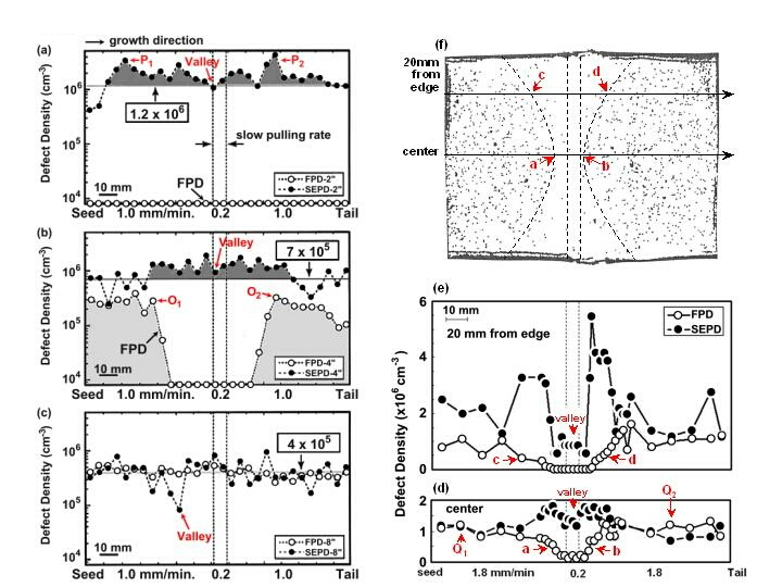
3. Discrepancies of the distributions of interstitials between the experimental and the simulation results Using the each neighboring wafer of the lifetime measurements, the densities of the FPD and the SEPD were counted along the center lines indicated by the arrows in Figs. 1 (a), (b), (c) and their density distributions were shown in Figs. 4(a), (b), (c), respectively. The FPD distribution shows the flow pattern to spread from a void [4] to the upper side when the wafer was put vertically in etchant.
Fig. 4. Density distributions of FPD and SEPD measured along center lines of three wafers in Fig. 1(a), (b) and (c). Other examples of valley phenomenon are Fig. 4(d) and (e). Growth conditions of Fig. 4(e) and (d) are the same as that of Fig 1(b) except pulling rate (1.8 mm/min). Pulling rate of Fig. 1(b) is 1.0 mm/min. Fig. 4(d) and (e) are FPD and SEPD density distributions along center line and 20 mm from edge line, respectively. (f) is COP map measured by LS-6000 (Hitachi). COP is revealed by NH4OH/H2O2 solution which is one of solution of RCA cleaning for 20 min and particle size counted is in the range of 0.1μm~0.13μm. a’, b’, c’ and d’ in Fig. 4(f) are corresponding to a, b, c and d in Fig. 4(d), (e), respectively. The original pits of the voids with the exaggerated flow pattern are only counted, therefore there is no chance to count the SEPD as the FPD. On the other hand, the size of the SEPD is so small in μm order, so the SEPD was separately counted using 10 times higher magnification [1] than that of the FPD. The one of the example of the SEPD pit was observed by AFM as shown in Fig. 5(b). 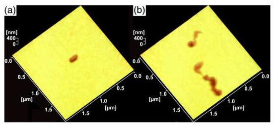
Fig. 5. (a) shows AFM images of a SF on ellipsoidal SF band, and (b) parts of interstitial type dislocation loops at inner part of ellipsoidal SF band in Fig. 1(a). It was shown from the observation that SEPD corresponds to interstitial type dislocation loops with irregular shape [2]. The two points of the discrepancies between the experiments and the simulation are described as follows: First, in Fig. 4(a) of the 50 mm diameter crystal, it was found that the P1 and P2 peaks of the maximum densities of the SEPD consist of only stacking faults (SF) and correspond to P1 and P2 on the red ellipsoidal band in the lifetime map of Fig. 1(a), respectively. This shows that the points of the minimum lifetime correspond to those of the maximum density of the SEPD on the SFB (band). The SFB consists of only the SF which have a disk-like shape with a interstitial type dislocation loop to be surrounded by the dangling bonds. The existence of the SF’s is confirmed not only by an optical microscope but also by AFM as shown in Fig. 5(a). On the crystal of 50mm in diameter, SEPD density was very high, but FPD density was nearly zero as shown in Fig. 4(a). This results show that the points P1 and P2 in Fig. 1(a) existed not in the V region but in the I region because the SF with dislocation loop is formed by the interstitials in the I rich region and the dangling bonds of the dislocations are the cause of the minimum lifetime. On the other hand, in the simulation by Dornberger et al. [8] shown in Fig. 1(a’) the both positions corresponding to P1 and P2 exist in the V rich region in Fig. 1(a’). Also, this region is the outside of the diffused region of and far away from the growth interface that is only the source and the reservoir of interstitials. However, the experimental results showed that the SF density is of 3~4 x 106 cm-2 at these positions and the crystal has not vacancies to be confirmed by the zero density of the FPD as shown in Fig. 4(a). From the result described above, it is clear that there is the decisive discrepancy between the experimental and the simulation results. Second, as shown in Figs. 1(a’) and (b’) in the simulation, the low pulling rate region colored by blue indicates the maximum densities of interstitials by the boundary condition from Voronkov’s model [9] that only the growth interface is the source and the reservoir of interstitials. However, the experimental results at the interface B including the SFB in Fig. 1(a) showed clearly not the maximum interstitial densities but rather depressed region denoted as “valley” in Fig. 1(a) and (b). Such interstitial depression distribution is also confirmed by the depressions of the SEPD densities as shown in the center region of Figs. 4(a) and (b). The depression region appeared not only in the 50 mm and 100 mm crystals but also in 200 mm crystal as shown by the growth interface B which is the concave shape with blue color in Fig. 1(c) and the corresponding minimum density of the SEPD in Fig. 4(c). This valley phenomenon by the low pulling rate was also reproduced by the other experiments as shown in Figs. 4 (d) and (e) and was shown in Fig. 2 in Roksnoer’s paper [10] again. Figures 4(d) and (e) show clearly the valley phenomenon in the distributions of the SEPD of the 100 mm crystal along to the center line and 20 mm line from the edge, respectively. The growth parameters of this crystal were the same as those of the crystal of Fig. 1(b) except the higher stationary pulling rate of 1.8 mm/min instead of 1.0 mm/min. The average FPD densities in the outside region of Q1 and Q2 in Fig. 4(d) and (e) had the same value of 1 x 106 cm-3 , and this value was about three times higher than 3 x 105 cm-3 in Fig. 4(b). These results show that the FPD density depends on the pulling rate. The depleted FPD densities in Fig. 4(d), (e) are considered the effect of recombination with the increased SEPD due to the low pulling rate. A typical type of such recombination effect was also observed in the depression(from O1 to O2) of the FPD densities by the increasing of the SEPD densities due to the low pulling rate in Fig. 4(b). The depleted distribution of the FPD in Fig. 4(d) was also reconfirmed by the measurement of COP’s (crystal originated particle) [11] using a particle counter. The COP is a void on a mirror- polished wafer which is the same as that of FPD [4]. The map of the COP in Fig. 4(f) was obtained from a neighboring mirror-polished wafer after so-called RCA cleaning. In the COP map each black point shows a scattered light point from a void. The positions of a, b in Fig. 4(d) and c, d in Fig. 4(e) correspond to the positions of a, b on center line and c, d on 20 mm from edge line in Fig. 4(f), respectively. In the simulation for the region of the low pulling rate, the interstitial density had the maximum as reservoir for interstitials [8] as seen from Figs. 1(a’) and 1(b’). However, it was showed from the experimental results on the COP that the region of the maximum interstitial density in the simulation corresponded to that of the minimum interstitial density as described by the valley phenomenon. The FPD distributions in Fig. 4(d), (e) were reconfirmed by the COP distribution in Fig. 4(f). The speculated interstitial distribution to be deduced from the experimental results give the reverse distribution of that in the simulation. Hence, it is impossible for the simulation to give the experimental secondary defect distribution. Moreover, from AOP analyses [12, 13, 14] of the detaching experiments on crystals we clearly demonstrated that the growth interface is always filled with vacancies. The same result was also reported by Roksnoer in the detaching experiment of the pedestal crystals [10]. It will be reported in detail at the conference . 4. Conclusions We showed that there are the many discrepancies between the point defects distribution by the simulation and the speculated point defect distribution by the analyses of experimental secondary defects as FPD, SEPD, COP, and AOP. Also, by the crystal detaching experiments from the melt, it is showed that the growth interface is always filled with vacancies. This shows that the growth interface is not the source and the reservoir of interstitials at the least. Moreover, Considering that the simulation is based on Voronkov’s model, the discrepancies show that Voronkov’s model itself is not suitable for the behavior of the intrinsic point defects in silicon crystals grown from the melt. References [1] T. Abe, K. Hagimoto, Proceedings of the Second International Symposium on Adv. Sci. and Tech. of Silicon Mat., 1996, p. 242. [2] T. Abe, Materials Science and Engineerings, B73 (2000) 16. [3] H. Yamagishi, I. Fusegawa, N. Fujimaki, M. Katayama, Semicond. Sci. Technol. 7 (1992) A135. [4] M. Itsumi, H. Akiya, T. Ueki, M. Yamawaki, J. Appl. Phys. 78 (1995) 5984. [5] M. Nishimura, Y. Yamaguchi, K. Nakamura, J. Jablonski, M. Watanabe, in: C.L. Cleays, P. Ray-Chauduhury, M. Watanabe, P. Stallhofer, H.J. Dawson (Eds.), High Purity Silicon V, The Electrochem. Soc. Ser. 98-13, Pennington, NJ, 1998, p.188. [6] S. Sadamitsu, S. Umeno, Y. Koike, M. Hourai, S. Sumita, T. Shigematsu, Jpn. Appl. Phys. 32 (1993) 3675. [7] H. Foell, B.O. Kolbesen, Appl.Phys. 8 (1975) 319. [8] E. Dornberger, W. von Ammon, J. Virbulis, B. Hanna, T. Sinno, J. Cryst. Growth 230 (2001) 291. [9] V.V. Voronkov, J. Cryst. Growth 59 (1982) 625. [10] P.J. Roksnoer, J. Cryst. Growth 68 (1984) 596. [11] J. Ryuta, E. Morita, T. Tanaka, Y. Shimanuki, Jpn. J. Appl. Phys. 29 (1991) L1947 [12] H. Harada, T. Abe, J. Chikawa, in: H.R. Huff, T. Abe, B.O. Kolbesen (Eds.) Semiconductor Silicon 1986, the Electrochem. Soc., Pennington, NJ, 1986, p. 76. [13] T. Abe, T. Takahashi, J. Cryst. Growth 334 (2011) 16. [14] K. Shirai, T. Abe, J. Cryst. Growth 351 (2012) 141. |
| Legal notice |
|
| Related papers |
Presentation: Oral at 17th International Conference on Crystal Growth and Epitaxy - ICCGE-17, General Session 7, by Takao AbeSee On-line Journal of 17th International Conference on Crystal Growth and Epitaxy - ICCGE-17 Submitted: 2013-02-25 02:37 Revised: 2013-04-12 07:56 |