| Search for content and authors |
Defect and Strain Analysis of Selective GaAs Epitaxy in STI Patterned Si (001) Substrate |
| Sun-Wook Kim 1, Young-Dae Cho 1, Won-Kyu Park 2, Chan-Soo Shin 2, Dae-Hyun Kim 3, Dae-Hong Ko 1 |
|
1. Yonsei University (Yonsei UNIV.), Sinchon-dong, Sudaemoon-ku, Seoul 120-749, Korea, South |
| Abstract |
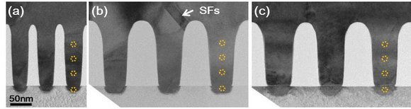
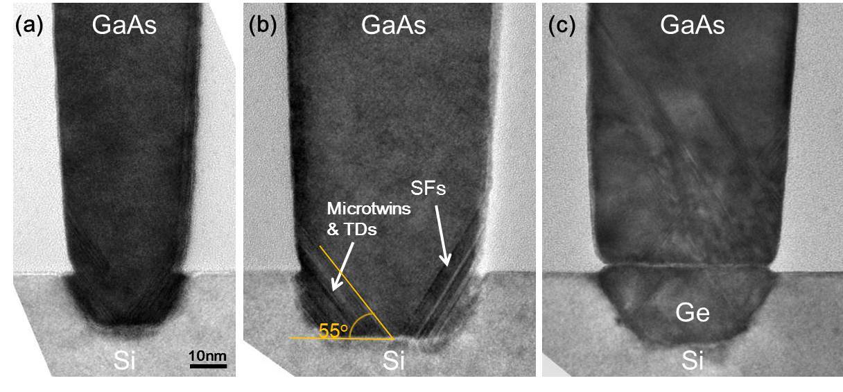
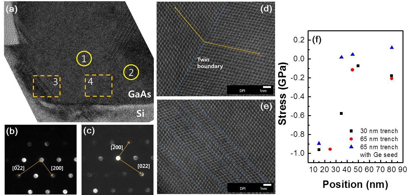
It is believed that the introduction of III-V materials in CMOS technologies needs to take advantage of the mature Si based technologies [1]. Among the significant progress in reducing the defect density in epitaxial GaAs grown on Si substrates, the selective epitaxial growth of the lattice mismatched materials in high aspect ratio trenches is well investigated route involving the elimination of dislocations by trapping of threading dislocations within trenches [2,3]. In this study, we carried out the epitaxial growth of GaAs layers in shallow trench isolation (STI) structures patterned on (001) Si substrates. The trench widths were 30 nm and 65 nm, and STI depths were 145 nm. The GaAs layer was deposited by metalorganic chemical vapor deposition (MOCVD) at 450~670°C. Patterned Si substrates with a Ge seed layer were also used to reduce the lattice mismatch between GaAs and Si. The microstructure and the channel strain were characterized using several techniques of TEM (JEOL, JEM-2100F) including nanobeam diffraction (NBD). The spatial resolution of NBD method was estimated to be around 2 nm with 0.1% strain resolution [4]. The TEM samples were fabricated using a focused ion beam (FIB) with 100 nm thickness. Figures 1 show the low magnification TEM cross-sectional images of GaAs layers in trenches of 30 nm (Fig. 1(a)), 65 nm (Fig. 1(b)) widths, and 65 nm widths with Ge seed layers (Fig. 1(C)). In all the samples, the TEM image shows that all of the trenches are well filled with a GaAs layer and the defect free region is observed near the top region of the trench, except the stacking faults originating from the top oxide layer, and boundaries in the overgrown regions. This result indicates that the dislocations originating at the GaAs/Si or GaAs/Ge interface were trapped within trench region. Figures 2 are the high resolution TEM images of GaAs layers for each sample. For the case of the samples without Ge seed layer, the threading dislocations, micro-twins and stacking faults are clearly observed forming an about 55°angle with the [11] direction. <110>-oriented threading segments would all be inclined to the (11) oxide sidewalls in <110> {111} slip system [2]. The dislocations from the GaAs/Si interface terminate at the oxide sidewall within 50 nm heights. On the contrary, defect formation becomes more pronounced in GaAs layers with Ge seed layer due to the presence of interfacial oxide layer between Ge and GaAs, and the defect free region is shown above 70 nm from the GaAs/Ge interface. In order to investigate the defects near the GaAs/Si interface, STEM and NBD measurements were performed. Figure 3(a) shows the HRTEM images of GaAs layers in 65 nm trench, and the STEM images from selected areas (Figs. 3(d) and 1(e)) reveal the twin boundary and micro-twins, respectively. NBD patterns obtained from each side of twin boundary clearly show that this twin structure is constructed by (11) mirror reflection or 180O rotation around the [111] axis. The stress distributions acquired from spots as denoted by yellow circle in Fig. 1 are plotted in Fig. 3(f). In the samples without a Ge seed layer, the graphs indicate that more compressive stress is induced in GaAs layers along the [110] direction at the bottom of trenches due to the smaller lattice constant of Si. The compressive stress gradually decreases up to the almost relaxed state near the top level of STI oxide. In the samples with a Ge seed layer, however, the compressive stress is induced only within a Ge seed layer and it seems that the GaAs layer is fully relaxed due to the high defect density. In addition, it is considered that the remaining compressive stress in GaAs layers is resulted from the STI oxides because STI oxide could act as a pedestal retarding the strain relaxation of GaAs layers. References 1. M. M. Heyns, M. Meuris, and M. Caymax, ECS Trans. 3 (2006), p. 511. 2. J. Bai, J.-S. Park, Z. Cheng, M. Curtin, B. Adekore et al, Appl. Phys. Lett. 90 (2007), p. 101902. 3. J. Z. Li, J. Bai, J.-S. Park, B. Adekore, K. Fox et al, Appl. Phys. Lett. 91 (2007), p. 021114. 4. J.-H. Yoo, S.-W. Kim, S.-M. Koo, D.-H. Ko, and H.-J. Lee, Appl. Phys. Lett. 98 (2011), p. 133121. Figure 1 Low magnification TEM cross-sectional images of GaAs layers in trenches of (a) 30 nm, (b) 65 nm widths, and (c) 65 nm widths with Ge seed layers.
Figure 2 High resolution TEM images of GaAs layers in trenches of (a) 30 nm, (b) 65 nm widths, and (c) 65 nm widths with Ge seed layers.
Figure 3 NBD patterns ((b), (c)), and STEM images ((d), (e)) from selected areas in (a) confirm the twin boundary and micro-twins. (f) The stress distributions acquired from spots as denoted by yellow circle in Fig. 1 using NBD method. |
| Legal notice |
|
| Related papers |
Presentation: Oral at 17th International Conference on Crystal Growth and Epitaxy - ICCGE-17, Topical Session 4, by Sun-Wook KimSee On-line Journal of 17th International Conference on Crystal Growth and Epitaxy - ICCGE-17 Submitted: 2013-04-15 15:37 Revised: 2013-07-18 12:33 |