| Search for content and authors |
Grain and Subgrain Boundaries in Multi-Crystalline Silicon |
| Eva-Regine Carl 1, Andreas Danilewsky 1, Arne Croell 1, Tobias Geiger 2, Elke Meissner 2 |
|
1. Kristallographie, Universität Freiburg (KI), Hermann-Herder-Str. 5, Freiburg 79104, Germany |
| Abstract |
Multi-crystalline silicon is one of the most important photovoltaic materials. However, its microstructure lowers the efficiency of the cells with grain boundaries and highly dislocated areas acting as effective recombination centers. This is why the main challenge is to optimize the structural properties. For this, detailed knowledge about the formation of the microstructure is needed. Grain and twin boundaries in multi-crystalline silicon grown by directional solidification were analyzed by means of Electron Backscatter Diffraction (EBSD) and Synchrotron X-Ray Topography (SXRT). Two nearest neighbor samples of one column were analyzed in order to get information about the development of grain boundaries during crystal growth. Thereby, the emphasis was placed on the evolution of one selected and its neighboring grains. From the analysis of the EBSD data for the large angle grain boundaries and twins, it was found that the common interface of adjacent grains that forms the grain boundary is not correlated to the rotation axis that defines the type of boundary. The results show that the interfaces formed by lower symmetry operations are responsible for the trace of the grain boundary. In the samples, significant changes with respect to non-“straight line” twin boundaries were found during the growth process. Grain boundaries of this type were formed or eliminated very quickly, while other types of grain boundaries experienced only small changes. By means of SXRT, the microstructure of the analyzed grain shows numerous small-angle grain boundaries with angles in the range between 0.05 and 0.15 degrees, which is well below the EBSD angular resolution of about ± 0.5°. Fig. 1 compares a transmission X-ray topography and an etch pit density map of the same small angle grain boundary. The small tilt of only w = 9 arcsecs (fig. 1 a) results after etching in a line of etch pits of such a high density, that the pits becomes uncountable (fig. 1b). It will be shown, that the "dislocation clusters" proposed from etch pit patterns are small angle grain boundaries with angles of 0.01 – 0.18 degrees, corresponding to a minimum theoretical dislocation density of about 108 cm-2 responsible for such a tilt value. The experiments give evidence that the small-angle grain boundaries with larger angles extend, while the smaller ones vanished. This enlargement from 0.1° to 30° finally results in the formation of a twin boundary. 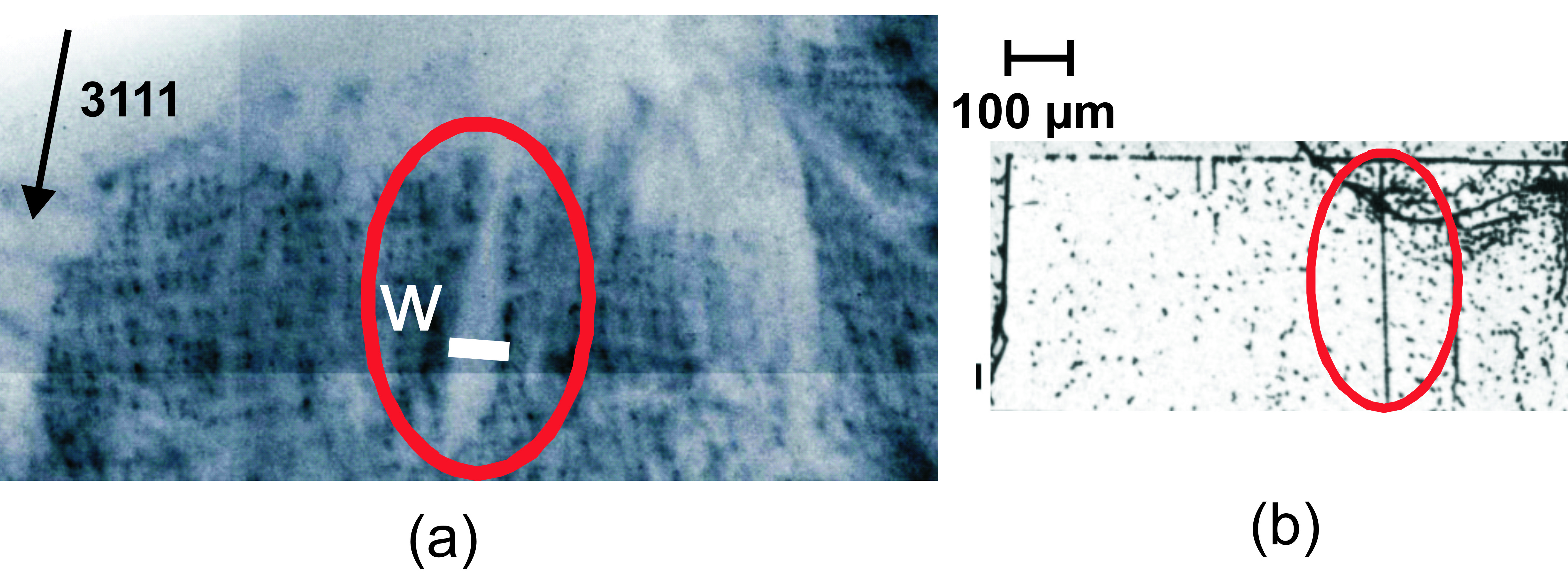
Fig. 1: Small angle grain boundary located in a single grain of mc-Si |
| Legal notice |
|
| Related papers |
Presentation: Oral at 17th International Conference on Crystal Growth and Epitaxy - ICCGE-17, General Session 7, by Eva-Regine CarlSee On-line Journal of 17th International Conference on Crystal Growth and Epitaxy - ICCGE-17 Submitted: 2013-04-14 13:37 Revised: 2013-07-09 22:17 |