| Search for content and authors |
Vapour phase growth of single crystalline GaN layers in hot microwave plasma |
| Radoslaw Zwierz , Sebastian Golka , Krzysztof Kachel , Dietmar Siche , Roberto Fornari |
|
Leibniz Institute for Crystal Growth (IKZ), Max-Born-Str 2, Berlin 12489, Germany |
| Abstract |
Gallium nitride (GaN) is already used as basic semiconductor for opto- and high frequency power electronics. The lack of cost effective bulk crystals drives the search for alternative growth methods to prepare homo-epitaxial substrates. We are using for Ga the Physical Vapor Transport (PVT) and microwave plasma for the N2 activation, to grow first layers on double side polished sapphire substrates. The main challenge is to improve the plasma process stability when interaction between microwaves and plasma does not allow accurate prediction of the desired microwave resonator adjustment at growth temperature. The spectra of Optical Emission Spectroscopy (OES) were utilized as markers for excitation efficiency, representing the operation parameters for controlled GaN growth in the metastable region of the phase diagram. Additionally, unfavorable vaporized impurities like Mo as cavity material can be detected, but there was no indication that it is sputtered. In contrast to spectra taken at RT, the lines of neutral and ionized molecules, N2* and N2+, and atomic nitrogen N could not be detected at growth temperature. Surprisingly, CN species were unambiguously detected, which means that reactive nitrogen was indeed present and reacted with carbon from insulation felt and susceptor graphite. The Ga related lines suggest that screening effects by Ga vapour and/or droplets do not severely affect the plasma formation. Figs. 1a and 1b show typical GaN layers after 4 h growth on sapphire and etching of excess Ga in HCl:H2O mixture (1:2). In case of sample (a), plasma was not burning steadily during the whole growth time and a large amount of Ga excess was found on the seed after the process. Ga catalyses GaN decomposition may hinder the coalescence of crystallites by in-situ etching action and leads to the formation of small pits on their top surface. The crystallites shown in Fig. 5b are smaller, without top surface pits and were grown without visible Ga excess. EDX maps confirmed that thecrystallites consist of GaN, but the carbon map showed some particle-like spots, which might be tiny dust from the surrounding graphite susceptor and isolation felt transported into the cavity by carrier gas. The full width at half maximum (FWHM) of high resolution X-ray diffraction (HRXRD) measurements was 0.60 deg (2160 arcsec). This high value is reasonable since crystal quality improves with layer thickness and stress relaxation after delamination from the sapphire substrate. 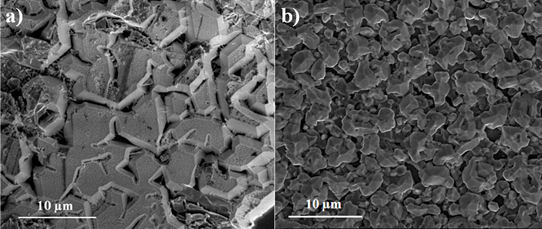
Fig. 1: Sample surfaces of GaN crystallites on sapphire grown with (a) and with no visible (b) Ga excess (SEM image) (Tsource = 1300°C, Tgrowth » 1000°C, p = 400 mbar, growth duration 4 h) |
| Legal notice |
|
| Related papers |
Presentation: Poster at 17th International Conference on Crystal Growth and Epitaxy - ICCGE-17, Topical Session 3, by Dietmar SicheSee On-line Journal of 17th International Conference on Crystal Growth and Epitaxy - ICCGE-17 Submitted: 2013-03-27 11:44 Revised: 2013-07-18 12:13 |