| Search for content and authors |
Nanofabrication - direct write and replication patterning technologies in EUMINAfab |
| Frank Dirne 1, Hans Loeschner 2, Manfred Kohl 3, Falco Delft 1, Elmar Platzgummer 2 |
|
1. Philips Research Laboratories, Prof. Holstlaan 4 WAG 12, Eindhoven 5656AA, Netherlands |
| Abstract |
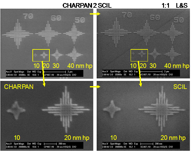
Nanodevice fabrication requires structuring techniques that, in an economically attractive way, can generate high-resolution features. Direct writing techniques, like electron- and ion-beam lithography, are slow and require very expensive machines. Hence, they are mostly used for nanodevice development. These techniques need scaling up by introducing the concept of massive parallel beams as is the case for CHARPAN (Charged Particle Nanopatterning) using 43-thousand programmable ion beams of 12.5nm beam size.
 |
| Legal notice |
|
| Related papers |
Presentation: Oral at EUMINAfab European research infrastructure for multimaterial micro and nano manufacture, by Frank DirneSee On-line Journal of EUMINAfab European research infrastructure for multimaterial micro and nano manufacture Submitted: 2010-06-23 17:42 Revised: 2010-08-19 12:08 |