| Search for content and authors |
GaAs/Al0.3Ga0.7As Quantum Dot Intermediate-band Solar Cell by Droplet Epitaxy |
| Sergio Bietti , Andrea Scaccabarozzi 1, Maurizio Acciarri , Stefano Sanguinetti 1 |
|
1. LNESS and Dipartimento di Scienza dei Materiali, Università di Milano-Bicocca, via Cozzi 53, Milano 20125, Italy |
| Abstract |
| Quantum dot intermediate band (IB) solar cells have been proposed in order to increase the efficiency of traditional solar cells and immediately attracted a lot of attention and research since the time they were first proposed [1]. The IB introduces an extension of the absorption coefficient of the semiconductor to lower energies, allowing a more thorough collection of the solar spectrum, via a two-step absorption of low-energy photons. Quantum dot (QD) structures are good candidates for IB solar cells, because their confined energy levels can overlap and form a miniband in dense arrays and the position of these levels and bands can be tuned varying the size and spacing of the QDs. The IB working mechanisms have been demonstrated for InAs QDs in GaAs [2], and a lot of research is devoted to reduce the problems due to strain, and defect nucleation increasing carrier escape [3]. Droplet epitaxy (DE) [4] is a molecular beam epitaxy technique that allows for the growth of quantum dots of materials lattice matched to the barrier and the removal of the wetting layer. DE makes possible to indipendently control density, size and shape of the nanostructures. Densities as high as some 1011 cm-2 per layer have been reported [5] and potentially a large number of layers can be stacked because the system is strain-free, leading to a much higher density of states in the IB than the more conventional Stranski-Krastanov techniques. Since it is a strain-free technique, there are virtually no defects in DE-grown materials, and this is fundamental to have high performance devices. Moreover, DE nanostructures can be grown without the presence of a wetting layer [6], that would introduce unwanted quantum-well-like states in the system. By tuning the size of the QDs it is obviously possible to change the position of the IB, and by tuning their aspect ratio the high energy states of the QDs can also be tuned in order to have a small electron-phonon coupling with the barrier. The lack of defect and wetting layer states can greatly reduce thermal escape of carriers from the IB, leaving photon-induced transitions the dominant ones, as requested by IB theory [1]. For these reasons DE is a good candidate for the realization of QD-IB solar cells. We demonstrate the key working principle of IB materials, that is the production of sub-gap two-photon photocurrent, with Al0.3Ga0.7
As solar cells containing GaAs QDs grown by DE (figure 1a). The devices were illuminated at 15K by continuous monochromatic light and chopped broadband IR light (1.5 – 20 μm), and the signal was demodulated by a lock-in amplifier. The continuous light pumps electrons into the QDs and the chopped IR promotes them to the CB where they can be collected generating an electric signal. As a control, a reference sample without QDs was grown and measured in the same conditions, but no two-photon signal was detected (see figure 2b). Measurements show that the shape of the two-photon photocurrent signal is different from the VB-CB photoresponse, indicating clearly that a two-photon process involving the QD levels is taking place. The two-photon signal response is in good agreement with the PL spectrum of the QD samples (figure 1b), that lets us easily understand the position of the energy levels of the system. [1] A. Luque, A. Martì, Physical Review Letters, 78, 5014 (1997). [2] A. Martì, E. Antolìn, C. R. Stanley, C. D. Farmer, N. Lòpez, P. Dìaz, E. Cànovas, P. G. Linares and A. Luque, Physical Review Letters 97, 247701 (2006). [3] A. Luque and A. Martì, Prog. Photovolt: Res. Appl. 9, 73-86 (2001) [4] N. Koguchi and K. Ishige, Japanese Journal of Applied Physics 32, 2052–2058 (1993). [5] M. Jo, T. Mano, Y. Sakuma and K. Sakoda, Applied Physics Letters 100, 212113 (2012) [6] S. Sanguinetti, K. Watanabe, T. Tateno, M. Wakaki, N. Koguchi, T. Kuroda, F. Minami, and M. Gurioli, Applied Physics Letters 81, 613 (2002). 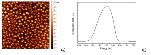
Figure 1: (a) AFM image of uncapped high density QDs grown by droplet epitaxy for the IB solar cell. (b) PL spectra of the QD sample at 15K with different excitation power. The QD emission energy indicates the IB energy level. 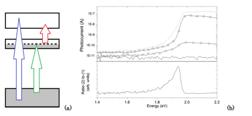 Figure 2: (a) Energy band diagram of the quantum dot solar cell with the main optical transitions outlined. (b) Upper panel: photocurrent signal of the QD and reference devices at 15K. Dashed curve is the AlGaAs reference cell single photon signal. Continuous, triangles and circles refer to the GaAs/AlGaAs QD photovoltaic cell: single photon signal (triangles), two-photon signal (circles) and noise level (continuous line). Lower panel: ratio of normalized two-photon to single-photon photocurrent signal, to better show the subgap photoresponse Figure 2: (a) Energy band diagram of the quantum dot solar cell with the main optical transitions outlined. (b) Upper panel: photocurrent signal of the QD and reference devices at 15K. Dashed curve is the AlGaAs reference cell single photon signal. Continuous, triangles and circles refer to the GaAs/AlGaAs QD photovoltaic cell: single photon signal (triangles), two-photon signal (circles) and noise level (continuous line). Lower panel: ratio of normalized two-photon to single-photon photocurrent signal, to better show the subgap photoresponse |
| Legal notice |
|
| Related papers |
Presentation: Oral at 17th International Conference on Crystal Growth and Epitaxy - ICCGE-17, General Session 8, by Andrea ScaccabarozziSee On-line Journal of 17th International Conference on Crystal Growth and Epitaxy - ICCGE-17 Submitted: 2013-04-15 23:43 Revised: 2013-07-26 09:07 |