| Search for content and authors |
Heteorepitaxy of high quality GaAs crystals on Silicon |
| Sergio Bietti 1, Andrea Scaccabarozzi 1, Roberto Bergamaschini 1, Monica Bollani 2, Emiliano Bonera 1, Claudiu Valentin Falub 3, Emanuele Grilli 1, Cesare Frigeri 4, Hans Von Känel 3, Leo Miglio 1, Stefano Sanguinetti 1 |
|
1. LNESS and Dipartimento di Scienza dei Materiali, Università di Milano-Bicocca, via Cozzi 53, Milano 20125, Italy |
| Abstract |
| In the quest for a viable path towards the monolithic integration of an quantum and optoelectronic devices onto a CMOS chip, we show that the recently developed approach for the hetero-epitaxial growth of Ge structures onto Si substrates [1], is also applicable to the GaAs on Si direct hetero-epitaxial growth. Fig. 1 shows an example of the three-dimensional hetero-epitaxy, namely GaAs micro-crystals (MCs), grown in a self-aligned manner on a periodic array of Si seeds. The seeds were formed by deep micro-machining of (001)-oriented, 6° off toward [110] Si substrates into pillars from 8 µm in height, with base width of 2 (not shown), 5 and 9 µm and spacing of 2 to 4 μm. Up to 8 μm of GaAs were deposited by MBE at a rate of 0.48 ML/s, a V/III ratio of 50 and a growth temperature of 580°C. This set of parameters was chosen to limit the diffusion length of Ga adatoms on GaAs, thus driving the growth toward kinetic limited morphologies. Depending on the choice of substrate pattern and the amount of material deposited, the arrays visible in Fig. 1 can cover almost the entire substrate surface, resulting in a measured space fillings of 90%. By preventing the formation of a continuous layer, crack propagation and wafer bowing are inhibited, even at large thickness GaAs deposit. An enlarged SEM image of the a GaAs crystal grown on Si pillars in shown in Fig. 1, in the case of pillar base width of 5 µm. The deposition is highly non-conformal, characterized by limited lateral expansion. The GaAs MC top is limited by clearly defined facets, with an anisotropy between the (110) and (1-10) directions due to the substrate miscut. The TEM analysis of the 5X5 2μm sample (Fig. 2) shows the presence of defected zones at the GaAs/Si interface and at the periphery of the crystal (Fig. 2), the latter characterized by the presence of stacking faults and threading dislocation arms. Due to 3D geometry of the deposit, such defects are readily expelled at the crystal sides. Antiphase domains are annihilated within few hundreds of nanometers from the interface. The topmost part of the GaAs MC, according to Raman measurements, appears completely relaxed. In order assess the GaAs crystal quality removing any interference from the low-quality material grown at the GaAs/Si interface, we realized GaAs crystals on Si pillars with an GaAs/AlGaAs heterostructure at the top, constituted by 200 nm of Al0.3Ga0.7
As topped with 300 nm of GaAs. For comparison, the same heterostructure was realized on GaAs-SI substrates (reference). The optical quality of the GaAs in the MC is confirmed by the intense room temperature emission, comparable to that of the GaAs bulk sample (Fig. 2c). The effect of growth conditions, pillar edge length and GaAs deposit thickness on the III-V material quality will be discussed. [1] C.V. Falub et al., Science 335, 1330 (2012). 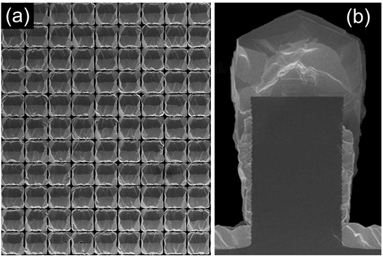 Figure 1: Panel (a): SEM top view of MC array obtained by heteroepitaxy of 8 μm of GaAs on Si patterned substrates (9×9 μm2 pillars with 4 μm trenches). Panel (b): SEM cross section of a single GaAs/Si pillar structure (5×5 μm2 pillars with 4 μm trenches). Dark areas correspond to Si. Figure 1: Panel (a): SEM top view of MC array obtained by heteroepitaxy of 8 μm of GaAs on Si patterned substrates (9×9 μm2 pillars with 4 μm trenches). Panel (b): SEM cross section of a single GaAs/Si pillar structure (5×5 μm2 pillars with 4 μm trenches). Dark areas correspond to Si.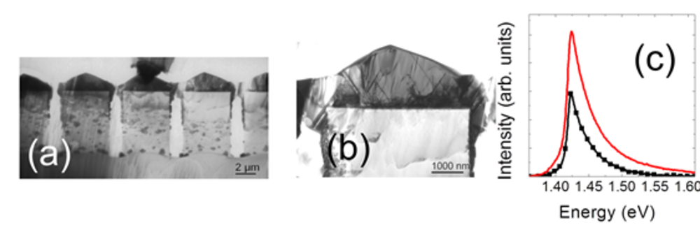 Figure 2 Panel (a): TEM images of MCs (2 µm thick GaAs on 5×5 µm2 pillars, 2 μm trenches). Panel (b): Image of a single MC. Panel (c) Room Temperature photoluminescence of Bulk GaAs (Black dots) and GaAs MC (4μm) Figure 2 Panel (a): TEM images of MCs (2 µm thick GaAs on 5×5 µm2 pillars, 2 μm trenches). Panel (b): Image of a single MC. Panel (c) Room Temperature photoluminescence of Bulk GaAs (Black dots) and GaAs MC (4μm) |
| Legal notice |
|
| Related papers |
Presentation: Oral at 17th International Conference on Crystal Growth and Epitaxy - ICCGE-17, General Session 10, by Stefano SanguinettiSee On-line Journal of 17th International Conference on Crystal Growth and Epitaxy - ICCGE-17 Submitted: 2013-04-15 23:30 Revised: 2013-07-25 11:56 |