| Search for content and authors |
3-dimensional InAs island growth on GaAs(001) at 500 oC observed by STMBE system |
| Takashi Toujyou , Teruki Teraoka , Shiro Tsukamoto |
|
Anan National College of Technology, Anan 774-0017, Japan |
| Abstract |
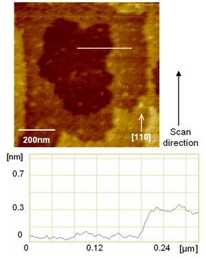
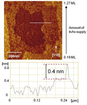
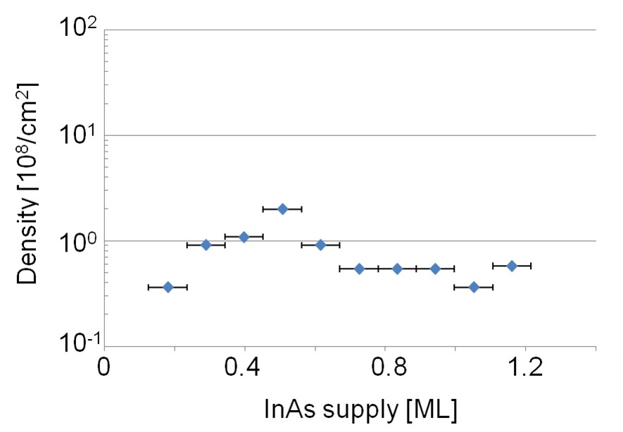
Quantum dots (QDs) are unique nano structures that have received special attentions in recent years because these are strong candidates for advanced semiconductor quantum devices. From recently reports, 3-dimensional (3D) islands (between InAs QDs and 1ML high InAs 2-dimensional (2D) islands) were formed during the QD formation [1, 2]. But, the precise mechanism for forming the 3D islands was not well understood yet. In this report, we observed the InAs 3D islands grown by the STMBE system [3] which equipped with a scanning tunneling microscope (STM) inside a molecular beam epitaxy (MBE) growth chamber, performing true in situ imaging during the MBE growth [4]. Fig.1 STM image and line profile. (a) STM image of before InAs supply, (b) line profile indicated as a white line. Fig.2 STM image and line profile. (a) STM image of during InAs supply, (b) line profile indicated as a white line. Fig.3 Densities of InAs 3D islands on GaAs(001) as a function of InAs supply. [1] D.Tex and I.Kamiya, Phys. Rev. B. 83, 081309 (2011). |
| Legal notice |
|
| Related papers |
Presentation: Oral at 17th International Conference on Crystal Growth and Epitaxy - ICCGE-17, General Session 6, by Takashi ToujyouSee On-line Journal of 17th International Conference on Crystal Growth and Epitaxy - ICCGE-17 Submitted: 2013-04-15 10:06 Revised: 2013-07-19 23:41 |