| Search for content and authors |
The epitaxial growth of Ge/Si structures on SiGe/Si(001) strain-relaxed buffers: transition from planar to island growth mode |
| Alexey V. Novikov 1, Mihail V. Shaleev 1, Dmitrij V. Yurasov 1, Dmitry N. Lobanov 1, Zaharij F. Krasilnik 1, Oleg A. Kuznetsov 2, Jean-Michel Hartmann 3 |
|
1. Institute for Physics of Microstructures Russian Academy of Sciences (IPM RAS), GSP-105, Nizhny Novgorod 603950, Russian Federation |
| Abstract |
The SiGe/Si(001) strain relaxed buffers can be used as templates for fabrication of various electronic and optoelectronic devices [1-4]. Control of strain in different layers of the structure grown on relaxed buffer provides significant bandgap engineering freedom and clears the way for fabrication of strain-compensated superlattices. Formation of structures on relaxed SiGe buffer requires an understanding of features of their growth mechanism. In particular, the transition from planar to island growth mode has to be known exactly for different growth conditions. In this paper features of the 2D-3D growth mode transition for Ge/Si structures fabricated on SiGe/Si(001) relaxed buffers are studied. The influence of Ge content in buffers and of strain in different layers on the critical thickness of 2D growth of Ge film is investigated. Si1-xGex/Si(001) linearly graded relaxed buffers with Ge content up to 40% fabricated both by atmospheric and reduced pressure chemical vapor deposition were used as artificial substrates. Chemical-mechanical polishing (CMP) of grown buffer was used in order to reduce their surface roughness. The threading dislocation density in all SiGe relaxed buffer was less than 106 cm-2. Investigated SiGe structures were grown by solid source MBE at 6500C on such relaxed buffers. Determination of the critical thickness of 2D growth of Ge film (hc) was performed in situ using reflection high electron energy diffraction (RHEED) and ex situ by atomic-force microscopy (AFM). Deposition of the Ge film was interrupted immediately after the change of RHEED picture from “streaked” to “spotty,” which indicates the 2D-3D transition. At first sight, hc should be higher for pure Ge growth on SiGe relaxed buffer as compared with growth on Si(001) due to the smaller lattice mismatch between the deposited film and the substrate. However, the experimental investigations have demonstrated unexpected results that values of hc for Ge/SiGe growth are smaller than in the case of Ge/Si(001) growth under the same conditions (same temperature and growth rate) (fig. 1). Moreover hc for Ge growth on SiGe buffer demonstrates a rather weak dependence on the composition of buffers and, consequently, on the lattice mismatch [5]. The decrease of critical thickness is related with Ge segregation and higher roughness of SiGe buffers in comparison with Si(001) substrates. According to the calculation Ge segregation during the MBE growth of unstrained SiGe layer leads to accumulation of approximately 0.8-0.9 ML (1 monolayer (ML)=0.136 nm) of Ge on the surface. As a result, the experimental value of hc determined by RHEED during growth of pure Ge on relaxed buffer should be 0.8-0.9 ML smaller than the actual amount of Ge on the surface. AFM analysis of SiGe buffers revealed that, in spite of usage of CMP the surface roughness of the SiGe buffers was 2-3 times higher than that of Si(001) substrates. An increase in the surface roughness may also occur during the MBE growth of an unstrained SiGe layer on top of the relaxed buffer prior to Ge deposition [6]. In the Si/Ge system, a gradual roughening of the growing film surface may cause island formation [7]. The larger value of surface roughness in the case of direct deposition of Ge on SiGe relaxed buffer could be one of the reasons for the shift of the 2D-3D transition point to lower amounts of deposited Ge. The larger surface roughness of buffer with higher Ge content would then counter-balance the lower lattice mismatch between pure Ge and that buffer, resulting in a weak dependence of hc on buffer composition (Fig. 1b). 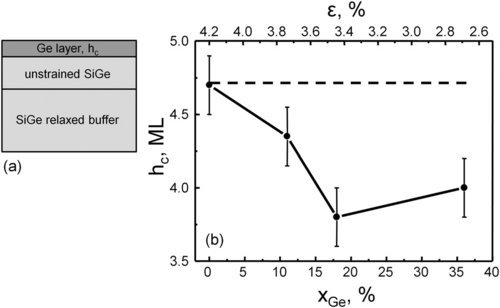
Fig. 1. a) - schematic view of the structures for investigation of the 2D-3D growth mode transition for direct Ge deposition on the SiGe/Si(001) relaxed buffer. b) - dependence of hc on the Ge content in SiGe buffer (bottom scale) and lattice mismatch (top scale) for Ge deposition on SiGe buffer. Dashed line corresponds to the hc value for Ge deposition on Si(001) substrates. It was obtained that hc of Ge film strongly depends on the thickness of tensile strained Si (sSi) layer deposited on the SiGe buffer before Ge growth (fig. 2). The value of hc is increased with the increase of sSi layer thickness and in the case of growth of Ge on pre-deposited sSi layers with thickness > 2 nm the critical thickness of 2D Ge growth is larger than in the case of growth of Ge on Si(001) substrates (fig. 2). The distinct dependence of hc on buffer composition is demonstrated in such structures. 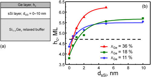
Fig. 2. a) - schematic view of the structures used for investigation of the 2D-3D growth mode transition for Ge growth on pre-deposited sSi layers. b) - dependences of hc on sSi layer thickness for the structures with different SiGe buffer composition. Dashed line corresponds to hc for Ge/Si(001) growth. Solid lines are guides for the eye. The obtained experimental results for Ge growth on sSi layers can be also explained by the Ge segregation and dependence of surface roughness on the sign and value of strain of layers grown on SiGe relaxed buffer [5]. On the one hand, the deposition of sSi layer and the increase of its thickness results in decrease of amount of Ge accumulated on the surface due to segregation. On the other hand, the deposition of thin tensile-strained Si layers on SiGe relaxed buffer indeed leads to gradual surface smoothing [8]. Both these factors lead to increase of the critical thickness of 2D growth of Ge with the increase of sSi layer thickness (fig. 2). It should be noted that for the sake of generality, the relaxed buffers fabricated by different methods were used in all experiments described above. Therefore, the obtained results cannot be connected with some technological features of the employed buffers. This work was supported by RFBR (grant # 13-02-01006-а), Scholarship for young scientists of the President of Russian Federation and programs of the Russian Academy of Sciences.
References: 1. M.L. Lee, E.A. Fitzgerald, M.T. Bulsara, M.T. Currie, and A. Lochtefeld. J. Appl. Phys., 97, 011101 (2005). 2. S. Tsujino, C.V. Falub, E. Müller, M. Scheinert, L. Diehl, U. Gennser, T. Fromherz, A. Borak, H. Sigg, D. Grützmacher, Y. Campidelli, O. Kermarrec, and D. Bensahel. Appl. Phys. Lett., 84, 2829 (2004). 3. Yu-Hsuan Kuo, Yong Kyu Lee, Yangsi Ge, Shen Ren, Jonathan E. Roth, Theodore I. Kamins, David A. B. Miller & James S. Harris, Nature 437, 1334-1336 (2005). 4. M. d’Avezac, Jun-Wei Luo, T. Chanier, A. Zunger, Phys. Rev. Lett. 108, 027401 (2012). 5. M.V. Shaleev, A.V. Novikov, D.V. Yurasov, J.M. Hartmann, O.A. Kuznetsov, D.N. Lobanov, Z.F. Krasilnik, Appl. Phys. Lett. 101, 151601 (2012). 6. K. Sawano, S. Koh, Y. Shiraki, N. Usami, and K. Nakagawa, Appl. Phys. Lett. 83, 4339 (2003). 7. J. Tersoff, B. J. Spencer, A. Rastelli, and H. von K€anel, Phys. Rev. Lett. 89, 196104 (2002). 8. Y. Bogumilowicz, J. M. Hartmann, N. Cherkashin, A. Claverie, G. Rolland, and T. Billon, Mater. Sci. Eng.: B 124–125, 113 (2005). |
| Legal notice |
|
| Related papers |
Presentation: Oral at 17th International Conference on Crystal Growth and Epitaxy - ICCGE-17, General Session 10, by Alexey V. NovikovSee On-line Journal of 17th International Conference on Crystal Growth and Epitaxy - ICCGE-17 Submitted: 2013-04-15 09:57 Revised: 2013-07-17 19:37 |