| Search for content and authors |
In-line accurate monitoring of pseudomorphic SiGe layers |
| Emmanuel S. Nolot 1, Jean-Michel Hartmann 1, Christophe Licitra , Denis Rouchon , Denis Renaud |
|
1. CEA-LETI-MINATEC (MINATEC), 17 rue des Martyrs, Grenoble 38054, France |
| Abstract |
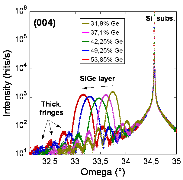
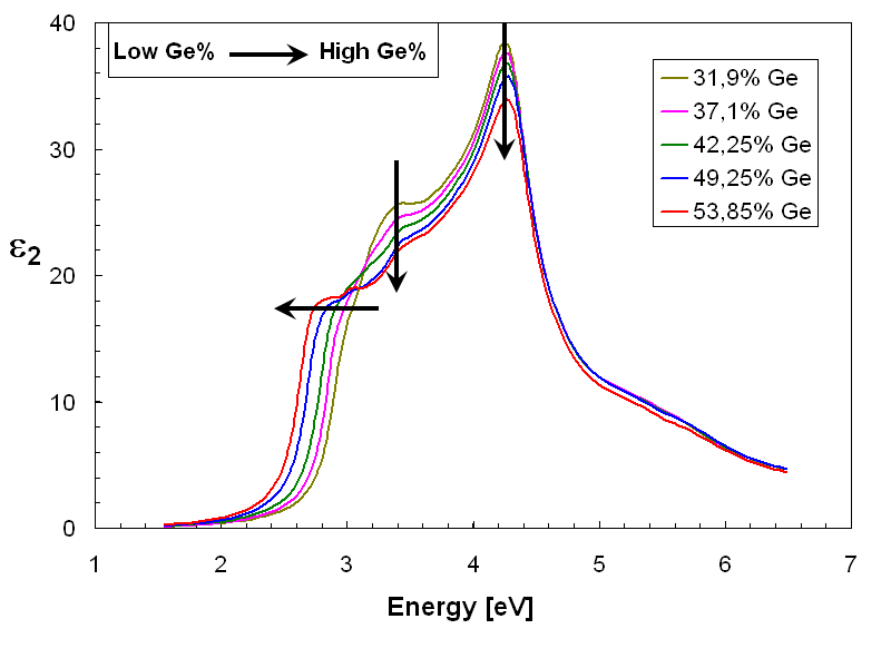
X-ray metrology techniques are quickly moving from characterization laboratories to semiconductor fabrication lines. They are now used to monitor Front End of the Line (FEOL) and Back End of the Line (BEOL) processes for the development of sub-45 nm technology nodes. Owing to their ability to determine thickness and elemental composition of thin films, as well as physical (crystallographic texture, density, porosity, roughness) and chemical (chemical bonding) properties of thin films and surfaces, they are more and more considered as at-line reference techniques, used to build calibration curves for other techniques (spectroscopic ellipsometry, etc) dedicated to fast in-line metrology on product wafers. Bandgap engineering by controlling either the strain or the Ge content significantly improves the performances of Si-based devices such as high performance Metal Oxide Semiconductor Field Effect Transitors (MOSFETs) etc. To meet the need of in-line accurate characterization of thin pseudomorphic SiGe layers, we used the following procedure. First, a set of SiGe layers with Ge contents in the 5 to 55% range were grown by Reduced Pressure Chemical Vapor Deposition (RP-CVD) on Si(001) substrates. In order to get smooth, pseudomorphic SiGe layers, both process temperature (550-750°C) and SiGe layer thickness (20-60 nm range) were decreased as the Ge content increased. Secondly, conventional ω-2θ scans around the (004) diffraction orders were performed on each samples (figure 1) using a Panalytical X’Pert high resolution diffractometer in order to precisely gain access to the Ge content. Then, SiGe layer thickness was determined by X-Ray reflectometry (XRR) with a convergent beam Jordan Valley JVX5200 tool. High-precision Variable Angle Spectroscopic Ellipsometry was then performed on a Woollam M2000 rotating compensator ellipsometer in the 190-1700 nm wavelength range. The SiGe dielectric function was calculated for each Ge contents, using XRR thickness as a reference. Based on these data, an alloy model (figure 2) was built and finally implemented on fast in-line ellipsometers for accurate determination of Ge content (in the 0-55% range) and thickness of pseudomorphic SiGe layers grown on 200 mm or 300 mm product wafers.
Figure1: ω-2θ scans around the (004) diffraction orders for pseudomorphic SiGe layers in the 31.9% to 53.85% Ge content.
|
| Legal notice |
|
| Related papers |
Presentation: Oral at 11th European Powder Diffraction Conference, Microsymposium 2, by Emmanuel S. NolotSee On-line Journal of 11th European Powder Diffraction Conference Submitted: 2008-04-11 09:12 Revised: 2009-06-07 00:48 |