| Search for content and authors |
Growth of corundum-structured α-(InxGa1-x)2O3 alloy thin films on sapphire substrates with buffer layers |
| Norihiro Suzuki 1, Kentaro Kaneko 1, Shizuo Fujita 2 |
|
1. Department of Electronic Science and Engineering, Kyoto University, Katsura, Kyoto 615-8510, Japan |
| Abstract |
Corundum-structured gallium oxide (a-Ga2O3), due to its expectably high breakdown electric field judging from wide band gap of 5.3 eV, is a novel candidate for high-voltage power devices as well as deep ultraviolet photonic devices. Band gap engineering is the basic requirements for heterostructure device applications, and has basically been achieved by alloying two or more binary semiconductors of the same crystal structure. We have showed the band gap engineering with a-(AlGa)2O3 from 5.3 to 7.8 eV for Al concentration from 0 to 0.81, keeping well-defined corundum structure [1]. The next target study is the band gap engineering with a-(InGa)2O3, which has been ready owing to our recent demonstration of a-In2O3 grown by the mist chemical vapor deposition (CVD) method [2]. The band gap engineering with these ternary alloys will be followed by the composition control of a-(AlGaIn)2O3 quaternary alloys, which will achieve a variety of heterostructures with unique properties, like (AlGaIn)N. In this presentation we will show the growth characteristics of a-(InGa)2O3 alloys. The growth of α-(InxGa1-x)2O3 was achieved by using α-Ga2O3 buffer layers on c-plane sapphire substrates by the mist CVD method, which is a safe technology with low energy consumption allowing the growth of high-quality α-Ga2O3 [3]. The growth temperature was 500 oC. The growth time of an α-Ga2O3 buffer layer and α-(InxGa1-x)2O3 were kept at 1 and 30 minute, respectively. Here gallium(III) acetylacetonate and indium(III) acetylacetonate were used as the sources of Ga and In, respectively. Fig.1 is the results of XRD measurement of α-(InxGa1-x)2O3 which has been grown by intentionally changing the In concentration x. The systematic shift of the XRD peaks suggests the successful growth of α-(InxGa1-x)2O3 alloy thin films with x = 0, 0.05, 0.08, 0.67. Fig 2 shows the band gap and resistivity in terms of the In concentration. The band gap was calculated from the transmittance of the films, and was moderately changed with x. The resistivities were calculated from the value of the sheet resistance meter. The drastic decrease of resistivity was confirmed by slight addition of In (x = 0.05, 0.08) to α-Ga2O3, suggesting significant enhancement of semiconductor properties without marked reduction of the band gap. At the conference the detailed electrical and optical properties of α-(InxGa1-x)2O3 alloy thin films will be shown to discuss their potential for wide band gap device applications.
References [1] H.Ito, K.Kaneko, and S.Fujita, Jpn. J. Appl. Phys. 51 (2012) 100207. [2] N.Suzuki, K.Kaneko, and S.Fujita, J. Cryst. Growth 364 (2013) 30. [3] D. Shinohara and S. Fujita, Jpn. J. Appl. Phys. 47 (2008) 7311.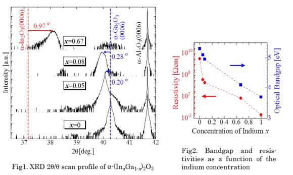 |
| Legal notice |
|
| Related papers |
Presentation: Oral at 17th International Conference on Crystal Growth and Epitaxy - ICCGE-17, Topical Session 3, by Norihiro SuzukiSee On-line Journal of 17th International Conference on Crystal Growth and Epitaxy - ICCGE-17 Submitted: 2013-04-11 11:52 Revised: 2013-07-18 11:21 |