| Search for content and authors |
Epitaxial growth of wide band gap oxide semiconductor thin films |
| Shizuo Fujita |
|
Photonics and Electronics Science and Engineering Center, Kyoto University, Katsura, Nishikyo-ku, Kyoto 615-8520, Japan |
| Abstract |
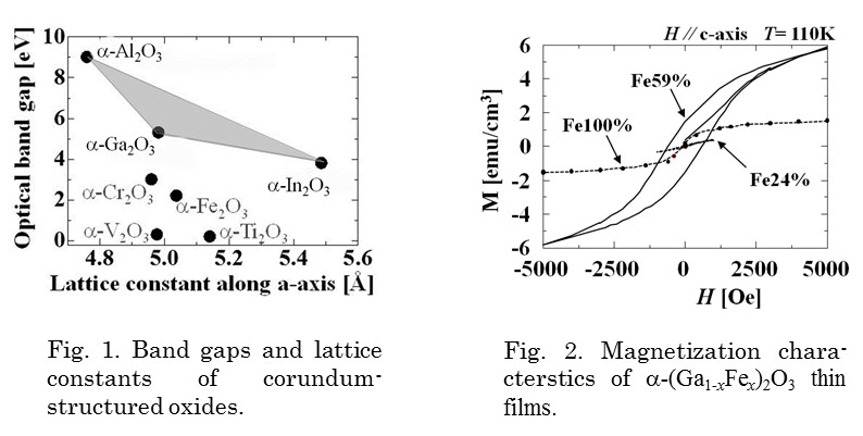
Wide band gap semiconductors are gaining increasing interest in order to meet the recent trends of such as high-power devices and UV light emitters. Exploration of new and novel materials has been the motive force for the development of the merging field. Oxide semiconductors have been recognized as low-cost and multifunctional materials since the evolution of ZnO-based semiconductors, and more recently, the target has been extended from II-O materials to III-O materials such as Ga2O3 and In2O3 owing to their unique properties. In this presentation, the up-to-date achievements on III-O materials, focusing on Ga2O3 and related alloys, will be summarized in order to call interest of participants on these materials as a possible candidate for next-generation new and novel devices. The researches Ga2O3 are now accelerating due to that highly-crystalline orthorhombic b-Ga2O3 substrates are available by solution methods and that its band gap is wider compared to GaN and SiC. Homoepitaxial growth by MBE has brought demonstration of Schottky diodes and MESFETs with high endurance against applied voltages[1,2], and is continuing to formation of MOSFETs. On the other hand, corundum-structured a-Ga2O3 is another target of the research, because orthorhombic crystals are rare in semiconductor family and there hardly are other semiconductors of the same crystal structure for alloys or multilayer structures with b-Ga2O3. We found that highly-crystalline corundum-structured a-Ga2O3, as evidenced by the very narrow w-scan x-ray diffraction FWHMs of 40-60 arcsec, can be formed on sapphire substrates by using the mist CVD growth method[3]. Doping of Sn realized n-type conductivity[4]. It should be noted that there are many corundum-structured crystals beside Ga2O3, as shown in Fig. 1. Band gap engineering is expected for the Al2O3-Ga2O3-In2O3 system, with which we may obtain semiconductor alloys with band gaps of 3.8-7.8 eV, similarly to the nitride semiconductor alloy system of AlN-GaN-InN. Composition (x) control of a-(AlxGa1-x)2O3 alloys from x=0 to 0.78 was successful, followed by the band gap tuning from 5.3 to 7.8 eV. For a-(InxGa1-x)2O3, single-phase alloys are at present made for the composition close to Ga2O3 or In2O3 and marked phase separation is seen for x between 0.2 and 0.6. It is interesting that the phenomenon is similar to InGaN at the early stage. Significant enhancement of conductivity for slight addition of In to a-Ga2O3 (x~0.05) is seen, suggesting enhanced semiconductor property without marked reduction in band gap. In addition to the above compounds, there are several transition-metal corundum-structured oxides, as shown simultaneously in Fig. 1. These compounds possess a variety of magnetic and electrical properties. Alloying or layering with Al2O3-Ga2O3-In2O3 alloys may create unique functions, that is, allow function engineering. For example, highly-crystalline alloys of a-(Ga1-xFex)2O3 were grown for the entire range of x from 0 to 1 keeping good crystallinity as highlighted by the w-scan x-ray diffraction FWHMs of smaller than 100 arcsec and no noticeable phase separation observed by TEM-EDX. As shown in Fig. 2, the a-(Ga1-xFex)2O3 films showed magnetization characteristics, more enhanced than Fe2O3. The hysteresis was as seen at room temperature for a-(Ga0.41Fe0.59)2O3 (Fe=59%). Doping of Sn increased the coercive force, suggesting enhanced spin-carrier interaction. Similar phenomena were also seen for a-(In1-xFex)2O3. New and multifunctional devices are expected by band gap engineering and function engineering of a variety of corundum-structured oxides. [1] K. Sasaki et al., Appl. Phys. Express 5, 035502 (2012), [2] M. Higashiwaki et al., Appl. Phys. Lett. 100, 013504 (2012), [3] D. Shinohara and S. Fujita, Jpn. J. Appl. Phys. 47, 7311 (2008), [4] K. Akaiwa and S. Fujita, Jpn. J. Appl. Phys. 51, 070203 (2012). |
| Legal notice |
|
| Related papers |
Presentation: Invited oral at 17th International Conference on Crystal Growth and Epitaxy - ICCGE-17, General Session 10, by Shizuo FujitaSee On-line Journal of 17th International Conference on Crystal Growth and Epitaxy - ICCGE-17 Submitted: 2013-04-14 13:37 Revised: 2013-07-17 20:41 |