| Search for content and authors |
Selective growth of (001) GaAs using patterned graphene mask |
| Yujirou Hirota , Yuya Shirai , Hiromu Iha , Yusuke Kito , Manabu Suzuki , Hironao Kato , Nao Yamamoto , Takahiro Maruyama , Shigeya Naritsuka |
|
Department of Materials Science and Engineering, Meijo University, 1-501 Shiogamaguchi, Tempaku-ku, Nagoya 468-8502, Japan |
| Abstract |
Selective growth is important not only for the fabrication of nanostructures but also the dislocation reduction in highly lattice-mismatched heteroepitaxy [1]. We have been studying selective growth of GaAs using molecular beam epitaxy (MBE) [2]. However, the window for the selective growth is very narrow because the selective growth is achieved by the re-evaporation of the adatoms on the mask. At the same time, the surface of the epitaxial layer becomes rough because of the high temperature of the growth. Therefore, a new material for the mask is requested to realize selective growth at low temperature. In this study, we focus on graphene as a mask material because graphene has two-dimensional structure and no bond towards the vertical direction. The critical temperature for the selective growth is firstly investigated with changing the growth temperature. Then, a pattered graphene mask is used to selectively grow GaAs. The critical temperature for the selective growth of GaAs on graphene was studied with changing the substrate temperature from 580 to 600oC. After finding the growth condition, the selective growth was performed on a patterned graphene mask, which was prepared by alcohol chemical vapor deposition (CVD). To form a patterned graphene mask, a 400nm-thick cobalt catalysis deposited by e-beam vapor deposition was firstly pattered into 7μm-wide stripes with period of 20μm using lift-off technique, as shown in Fig.1. Then, the graphene was grown by alcohol CVD on the Co catalysis. The CVD growth temperature and time was chosen to 450oC for 10 min. After forming the graphene mask, the selective growth of GaAs was performed using MBE. The growth temperature and the thickness of the layer were set at 600oC and 240nm, respectively. The grown layers were investigated using a scanning electron microscope (SEM). Figure 2 shows SEM plane-view images of the selectively grown GaAs layers on graphene masks. Though several small polycrystalline of GaAs are observed on the sample grown at 580oC, no polycrystalline are found on the graphene masks of the samples grown above 590oC. On the other hand, a lot of polycrystalline were occurred on the SiO2 mask even at 600oC (not shown in the figure). The result indicates that the critical temperature of the selective growth on graphene is lower than that on SiO2. The latter critical temperature is about 630oC [2]. The weak bonding characteristics of the graphene is thought to increase the re-evaporation and/or the surface migration of the Ga adatoms. Consequently, the selective growth is able to realize about 30oC lower on the graphene. The selective growth of GaAs on a patterned graphene mask is shown in Fig.3. This figure clearly shows that a superior selectivity of growth and an extremely flat GaAs layer were obtained by the selective growth with the pattered graphene mask at 600oC. The detailed mechanism of the growth using graphene will be discussed at the conference site. Acknowledgments This work was partly supported by Grant-in-Aid for Priority Area (B) No.22360131 from the Ministry of Education, Culture, Sports, Science, and Technology of Japan. Reference [1] For example, G.Bacchin and T.Nishinaga : J. Crystal Growth 208 (2000) 1-10. [2] S. Naritsuka, S. Matsuoka, Y. Yamashita, T. Maruyama, J. Crystal Growth, 310 (2008) 1571-1575. 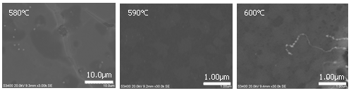 (a) (b) (c) (a) (b) (c)
Fig.2 GaAs selective growth on graphene 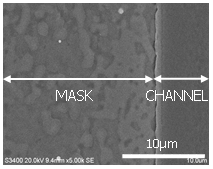
Fig.3 GaAs selective growth on patterned graphene |
| Legal notice |
|
| Related papers |
Presentation: Poster at 17th International Conference on Crystal Growth and Epitaxy - ICCGE-17, General Session 10, by Yujirou HirotaSee On-line Journal of 17th International Conference on Crystal Growth and Epitaxy - ICCGE-17 Submitted: 2013-04-09 04:17 Revised: 2013-07-17 22:22 |
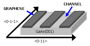 Fig.1 Patterned graphene mask for selective growth