| Search for content and authors |
c-plane GaN selective growth by liquid phase electroepitaxy under atmospheric pressure |
| Shigeya Naritsuka , Daisuke Kambayashi , Hiroyuki Takakura , Masafumi Tomita , Takahiro Maruyama |
|
Department of Materials Science and Engineering, Meijo University, 1-501 Shiogamaguchi, Tempaku-ku, Nagoya 468-8502, Japan |
| Abstract |
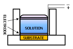
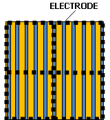
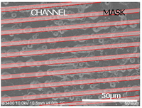
Sodium addition and high ambient pressure are mandatory to grow GaN in the conventional liquid phase epitaxy (LPE). To solve these difficulties, Hussy et al. proposed low-pressure solution growth (LPSG), where GaN is able to grow without the use of Na at atmospheric pressure [1]. The growth rate of LPSG is not high because the solubility of nitrogen is low. Therefore, liquid phase electroepitaxy (LPEE) was applied to improve the growth rate. On the other hand, the selective growth is useful not only for the fabrication of nanostructures but also the dislocation reduction in highly lattice-mismatched heteroepitaxy [2]. In this paper, LPEE is applied to selective growth of c-plane GaN layer using LPSG without the use of Na at atmospheric pressure. The lateral growth over the mask is also attempted by the technique. GaN template was used as a substrate. Straight line-openings with a width of 20μm and period of 40μm were cut into a W mask on the template substrate in the [11-20] direction. Using a mixture of Ga:Ge = 75:25 as a solution, LPEE was conducted under H2 ambient at atmospheric pressure. Other growth parameters were set as followings ; the growth temperature of 960oC, the growth time of 20h, the current flow of 4.0A, and the flow rate of NH3 mixed gas (NH3:H2 = 1:99) of 30.0sccm, respectively. The electrodes were immersed into the solution to flow electric current through the solution, as shown in Fig.1. In addition, the bottom electrode was contacted with the W mask on the substrate to uniformly flow the current. The shape and the arrangement of the bottom electrode are shown in Fig.2. A scanning electron microscope image of the selectively grown GaN layer is shown in Fig.3. The figure shows both a selective growth and a lateral growth was achieved. The white areas in the figure show the side slopes of the selective growth. Then, the area surrounded by the slope is the region where the W mask is appeared. It indicates an excellent selectivity of the growth was performed. On the other hand, a flat place with no white line over the W mask suggests the adjacent grown stripes met together to form a flat area. The lateral growth is thought to enhance by the increased density of the solute over the mask, which was caused by the current flow toward the W mask and the suppression of the growth on the mask. The detailed mechanism of the growth will be discussed at the conference site. Acknowledgements This work was supported by Grant-in-Aid for Priority Area (B) (No.22360131) from the Ministry of Education, Culture, Sports, Science and Technology of Japan. Reference [1] S. Hussy, E. Meissner, P. Berwian, J. Friedrich, G. Müller, J. Cryst. Growth 310 (2008) 738-747. [2] For example, G.Bacchin and T.Nishinaga : J. Crystal Growth 208 (2000) 1-10. Fig.1 Schematic of LPEE equipment Fig.2 Arrangement of electrode on substrate Fig.3 Selectively grown c-plane GaN layer using patterned W mask. The position of the mask are shown by the shaded areas. |
| Legal notice |
|
| Related papers |
Presentation: Oral at 17th International Conference on Crystal Growth and Epitaxy - ICCGE-17, Topical Session 3, by Shigeya NaritsukaSee On-line Journal of 17th International Conference on Crystal Growth and Epitaxy - ICCGE-17 Submitted: 2013-04-06 10:29 Revised: 2013-07-23 17:27 |