| Search for content and authors |
High resolution SEM imaging of non-conducting ceramics. |
| Sebastian Wachowski , Aleksandra Mielewczyk-Gryń , Maria Gazda |
|
Gdansk University of Technology, Faculty of Applied Physics and Mathematics, Narutowicza St. 11-12, Gdańsk 80-233, Poland |
| Abstract |
Scanning Electron Microscopy (SEM) is an useful and efficient technique for sample surface imaging. SEM micrographs can provide many useful information about sample microstructure, surface topography and in combination with Energy Dispersive X-ray Spectroscopy phase content. Novel SEM devices are able to image objects in nanoscale. However, in case of non-conducting materials high resolutions are hard to obtain and furthermore surface charge accumulation inhibits proper measurement. There are many ways for measuring non-conducting samples: fast image scanning, low electron beam voltage and current or performing measurements in low vacuum or low pressure environments. However, the easiest way to achieve sharp SEM image is coating the sample with thin layer of gold, platinum or carbon and thereby making sample conductive. In this work samples of arsenic doped lanthanum ortho-niobate non-conducting ceramics. Samples were sputtered with carbon or gold using LEICA EM SCD-500 sputter. Micrographs of uncoated sample and samples coated with carbon and gold were obtained using Quanta FEG 250 Scanning Electron Microscope by Everhart‑Thorney detector in high vacuum mode. Comparison of imaging quality of uncoated samples and coated samples were done. Figure 1 represents image of uncoated sample and Figure 2 depict sample coated with gold. Difference in image quality and resolution between Fig.1. and Fig.2. is clearly visible.
|
| Legal notice |
|
| Related papers |
Presentation: Poster at 15th Summer School on Crystal Growth - ISSCG-15, by Sebastian WachowskiSee On-line Journal of 15th Summer School on Crystal Growth - ISSCG-15 Submitted: 2013-07-03 13:08 Revised: 2013-07-03 14:02 |
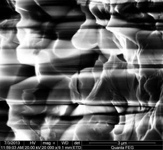 Figure 1. SEM image of uncoated LaNb0,8As0,2O4.
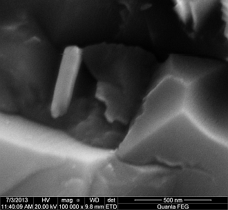 Figure 2. SEM image of Au-coated LaNb0,8As0,2O4.