| Search for content and authors |
Influence of synthesis temperature on SiC nanowires structure and shape |
| Marco Negri 1,2, Paola Lagonegro 1,2, Giovanni Attolini 1, Francesco Boschi 2, Matteo Bosi 1, Marco Campanini 1,2, Sathish Chander Dhanabalan 1, Filippo Fabbri 1, Francesca Rossi 1, Giancarlo Salviati 1 |
|
1. IMEM- CNR (IMEM), Parma, Italy |
| Abstract |
Silicon carbide is a wide band-gap semiconductor with high electron mobility, excellent thermal and mechanical properties. However the growth of SiC single crystal with low defect and impurities level is still an issue. On the contrary, SiC nanostructures are studied for nanocomposites, catalysis, and optics because they sum up nanostructured materials features coupled with the properties of silicon carbide; in addition, recently hydrogen storage capability have been demonstrated and they recently received much attention for their biocompatibility properties, making it possible to use them for highly sensitivebiosensor. In this work we report on the growth of cubic silicon carbide nanowires by means of vapour phase epitaxy using VLS growth mechanism. The nanowires have been grown in a VPE reactor heated by induction, at temperatures ranging from 1000° C to 1250° C. A 2 nm thick metallic layer (Ni) was deposited prior to growth by means of electron beam deposition, in order to act as a catalyst. The typical growth experiment involves two steps: thermal treatment (dewetting) to obtain a patterned distribution of metal, and finally epi-growth in mixtures of silane and propane. Morphology and structure of both dewetting stage and final growth results were characterized by Field Emission Gun Scanning Electron Microscope (FEG-SEM) (Jeol - 6400F) and Transmission Electron Microscope (TEM) (Jeol – JEM 2200 FS) was used for High-Resolution (HR-TEM) studies and High Angle Annular Dark Field imaging in Scanning mode (HAADF-STEM). The cubic SiC structure was confirmed by X-ray diffraction. With different growth temperatures there is an evident change in size, crystallographic structures and shape due to different stacking sequences of the silicon carbide atomic layers. TEM studies highlight different defects type and frequency varying growth temperature. Starting from this results, the growth process was optimized to obtain an enhanced control over nanowires shape and structure for several applications. 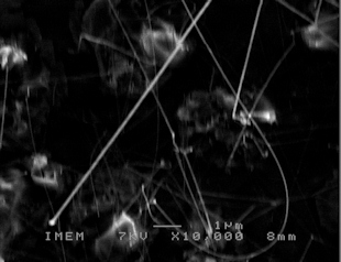 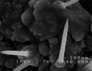 Fig. 1: effect of different growth temperatures on SiC nanowires structure (SEM image) |
| Legal notice |
|
| Related papers |
Presentation: Poster at 15th Summer School on Crystal Growth - ISSCG-15, by Marco NegriSee On-line Journal of 15th Summer School on Crystal Growth - ISSCG-15 Submitted: 2013-05-31 20:02 Revised: 2013-05-31 20:13 |