| Search for content and authors |
Epitaxial growth on porous substrates |
| Jan Grym 1, Peter Gladkov 1, Jan Vaniš , George P. Dimitrakopulos 2, Calliope Bazioti 2, Philomela Komninou 2, Eduard Hulicius 3, Jiří Pangrác 3, Oliva Pacherová 3 |
|
1. Czech Academy of Sciences, Institute of Photonics and Electronics, Chaberská 57, Prague 18251, Czech Republic |
| Abstract |
Integration of directly grown lattice-mismatched materials is hampered by the generation of misfit dislocations, which greatly affect performance, reliability and lifetime of semiconductor devices. A number of defect engineering approaches have emerged to gain control over the generation of defects during heteroepitaxial growth. One of the unconventional approaches is the use of porous substrates. We report on the electrochemical preparation of porous substrates of InP and GaAs and discuss specific problems related to their application in epitaxial growth from the liquid and vapor phase. We show that on porous substrates the onset of plastic relaxation can be avoided or shifted to larger layer thickness depending on the layer composition and correspondingly the lattice mismatch. The pore etching was carried out in an electrochemical cell using a three-electrode configuration. A home-made potentiostat/galvanostat was computercontrolled and allowed to register all process variables. The porous substrates and epitaxial layers were prepared by liquid phase epitaxy (LPE) and metal-organic vapor phase epitaxy (MOVPE) and were characterized by optical microscopy, scanning electron microscopy (SEM), focused ion beam microscopy (FIBM), cross sectional transmission electron microscopy (XTEM), atomic force microscopy (AFM), x-ray diffraction (XRD), and low temperature photoluminescence spectroscopy (PL). Porous substrates with low surface roughness and low density of pores in the nucleation layer (on the substrate surface, see Fig. 1) are appreciated to be easily laterally overgrown at an early stage of epitaxy; the pores should branch below this nucleation layer and thus allow for a high porosity and uniformity of a porous layer. This was achieved in highly concentrated HCl for InP substrates and HF-KI based electrolyte for GaAs substrates (Fig. 2). A set of samples of InGaAs/GaAs MOVPE experiments with a different composition of the ternary alloy (5, 10 and 20 % of In) and different thickness of the layer below and above the expected critical value on both porous and monolithic substrates was intentionally prepared for XRD and TEM measurements (Fig. 3). Significantly higher amount of elastic strain was retained in the layers deposited on porous substrates and the density of misfit dislocations was significantly reduced as compared to the layers grown on conventional substrates in the same growth run (Fig. 4). Work supported under the 2012-2014 Greece-Czech bilateral R&D collaboration project “III-V semiconductor heterostructures/nanostructures towards innovative electronic and photonic applications”. 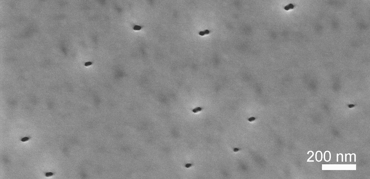
Fig. 1: SEM image of the surface of the low-roughness porous GaAs substrate 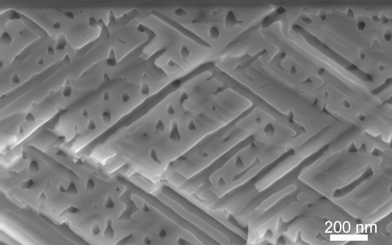
Fig. 2: SEM image of the cross-section of the lowroughness porous GaAs substrate 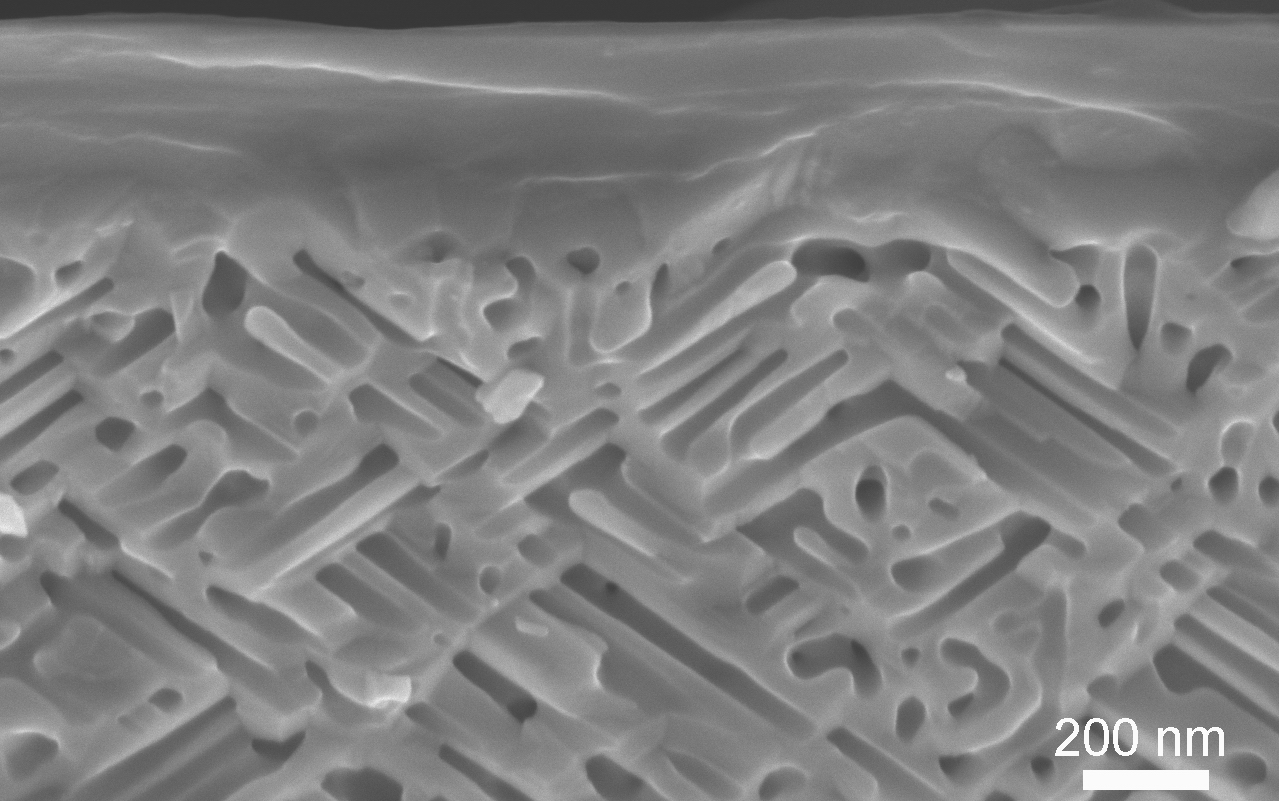
Fig. 3: SEM picture of the cross-section of the In0.2Ga0.8As/GaAs heterostructure grown by MOVPE on a porous GaAs substrate 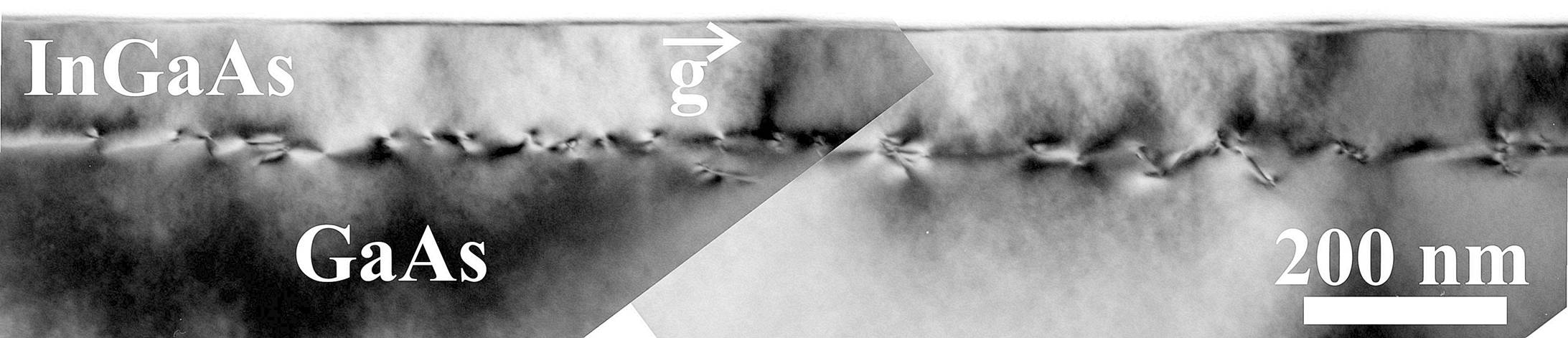 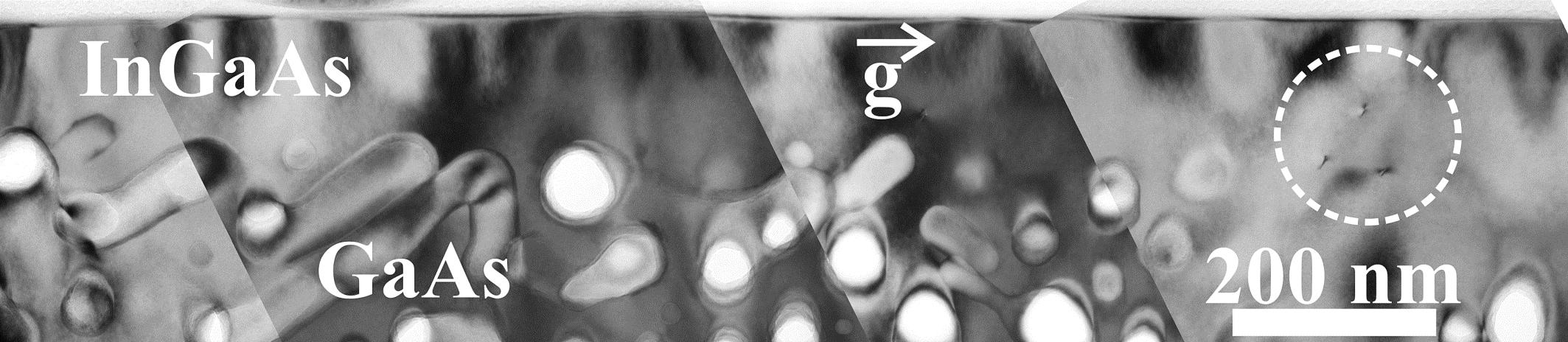
Fig. 4: Two-beam BF TEM image of the In0.2Ga0.8As/GaAs heterostructure grown using a conventional substrate (upper image) and a porous substrate (lower image) with epilayer thickness 100 nm. The image was taken near the [110] z.a. with g 2-20. The misfit dislocation density was reduced from 2.8x105 cm-1 to 1.2x104 cm-1. |
| Legal notice |
|
| Related papers |
Presentation: Poster at 15th Summer School on Crystal Growth - ISSCG-15, by Jan GrymSee On-line Journal of 15th Summer School on Crystal Growth - ISSCG-15 Submitted: 2013-05-21 17:43 Revised: 2013-05-21 18:14 |