| Search for content and authors |
From GaMnAs to CuMnAs: growth by Molecular Beam Epitaxy (MBE) |
| Richard P. Campion 1, P. Wadley 1,2, Vit Novak 2, C. Rinaldi 2,3, X. Martı 2,4,5, H. Reichlova 2,4, J. Zelezny 2, J. Gazquez 6, M. A. Roldan 7,8, M. Varela 7,8, D. Khalyavin 9, S. Langridge 9, D. Kriegner 10, F. Maca 11, J. Masek 11, R. Bertacco 3, V. Holy 4, A. W. Rushforth 1, K.W. Edmonds 1, B. L. Gallagher 1, C. T. Foxon 1, J. Wunderlich 2,12, T. Jungwirth 1,2 |
|
1. School of Physics and Astronomy, University of Nottingham, Nottingham NG72RD, United Kingdom |
| Abstract |
| The ferromagnetic semiconductor GaMnAs has proven to be a very successful prototype material that has enabled us to study the fundamentals of spintronics. In particular, a number of generally applicable concepts have been discovered in this material system, which can be readily applied to other ferromagnetic materials [1-3]. However, for successful device applications the Curie temperature must be well above room temperature and this does not seem likely to be the case in GaMnAs. Many groups are therefore looking for altenative options. Amongst the various options, antiferromagnetic materials in general seem to offer Neel temperatures in the appropriate temperature range. Antiferromagnets have long been key components in hard disk read heads, due to the exchange bias effect, while recent studies have demonstrated the potential of antiferromagnets as the active component in spintronics devices [4-8]. Our first studies involved the growth and characterisation of LiMnAs [7], which has an appropriate Neel temperature, but the inclusion of the alkali metal element represents a challenge both in terms of the growth and the stability of devices. However, LiMnAs is one of a family of antiferromagnetic I-II-V materials, which may be semiconductors or semi-metals, that could potentially be used for device applications. Here we report the epitaxial growth of a new high temperature antiferromagnetic material, tetragonal CuMnAs, which exhibits excellent crystal quality, chemical order and compatibility with existing semiconductor technologies. We demonstrate growth on the III-V semiconductors GaAs and GaP, and show that the structure is also lattice matched to Si in-plane. The CuMnAs was grown by MBE in a Veeco Gen III system using elemental sources for the Cu,Mn and the As. Extensive structrual characterisation has been performed including Z-contrast TEM, X-ray and neutron scattering: this data will be presented. CuMnAs is shown to be a collinear antiferromagnet with a high transition temperature. Layers capped with Fe are used to demonstrate a large and stable room temperature exchange bias. This material may offer new possibilities for spintronic applications combining antiferromagnetic and semiconducting materials. a) b) 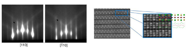
a) RHEED images of the surface of a CuMnAs layer during growth on a GaP substrate. b) Z-contrast TEM image of CuMnAs along the [1 0 0] direction. The As positions are clearly visible as the brightest atoms, and intensity analysis along the rows reveal a highly ordered compound in complete agreement with the overlaid model structure [1] Chiba, D.; Y. Sato, T. Kita, F. Matsukura, H. Ohno. "Current-Driven Magnetization Reversal in a Ferromagnetic Semiconductor (Ga,Mn)As/GaAs/(Ga,Mn)As Tunnel Junction". Phys. Rev. Lett. 93 (21): 216602. [2] Gould, C.; C. Ruster, T. Jungwirth, E. Girgis, G. M. Schott, R. Giraud, K. Brunner, G. Schmidt, L. W. Molenkamp. "Tunneling Anisotropic Magnetoresistance: A Spin-Valve-Like Tunnel Magnetoresistance Using a Single Magnetic Layer". Phys. Rev. Lett. 93 (11): 117203. [3] Giddings, A. D.; M. N. Khalid, T. Jungwirth, J. Wunderlich, S. Yasin, R. P. Campion, K. W. Edmonds, J. Sinova, K. Ito, K.-Y. Wang, D. Williams, B. L. Gallagher, C. T. Foxon. "Large Tunneling Anisotropic Magnetoresistance in (Ga,Mn)As Nanoconstrictions". Phys. Rev. Lett. 94 (12): 127202. [4] Park, B. G.; Wunderlich, J.; Marti, X.; Holy, V.; Kurosaki, Y.; Yamada, M.; Yamamoto, H.; Nishide, A.; Hayakawa, J.;Takahashi, H.; Shick, A. B.; Jungwirth, T. Nature Mat. 2011, 10, 347. [5] Martı, X.; Park, B. G.; Wunderlich, J.; Reichlova, H.; Kurosaki, Y.; Yamada, M.; Yamamoto, H.; Nishide, A.; Hayakawa, J.;Takahashi, H.; Jungwirth, T. Phys. Rev. Lett. 2012, 108, 017201. [6] Shick, A. B.; Khmelevskyi, S.; Mryasov, O. N.; Wunderlich, J.; Jungwirth, T. Phys. Rev. B 2010, 81, 212409. [7] Jungwirth, T. et al. Phys. Rev. 2011, B 83, 035321. [8] Cava, R. J. Physics 2011, 4, 7. |
| Legal notice |
|
| Related papers |
Presentation: Invited oral at 17th International Conference on Crystal Growth and Epitaxy - ICCGE-17, Topical Session 2, by Richard P. CampionSee On-line Journal of 17th International Conference on Crystal Growth and Epitaxy - ICCGE-17 Submitted: 2013-05-10 12:39 Revised: 2013-07-17 22:57 |