| Search for content and authors |
Structural and optical properties of GaPN(As) and InGaPN layers grown by MBE |
| Aleksandra Lazarenko , Ekaterina Nikitina , Evgeny Pirogov , Maksim Sobolev , Anton Egorov |
|
St Petersburg Academic University, Khlopina Str 8/3, S.Petersburg 194021, Russian Federation |
| Abstract |
Growing high-quality III–V compound semiconductors with a direct band-gap on Si substrates is the key to implementation of optoelectronic integrated circuits (OEIC) on Si substrates. Physicists have long wished to create a single chip, combining III–V compounds with Si. The main problem in the growth of III–V compounds on Si is the unwanted generation of structural defects such as dislocations, stacking faults and anti-phase domains. A large number of dislocations is formed during the growth of light emitting III-V compounds on Si substrates due to the large lattice mismatch [1]. GaP has almost the same lattice constant as Si, but has indirect band gap. This problem can be overcomed by growing III–V–N alloys which are lattice-matched to Si and has the direct band-gap [2]. Growing dislocation-free GaP(As)N and InGaPN layers with direct band-gap on GaP substrate is the first step of creating OEIC on Si [3,4]. We investigated optical and structural properties of GaP1-xNx bulk layers and In1-x-yGaPyNx and GaPyNxAs1-x-y quantum wells grown by molecular-beam epitaxy on GaP (001) substrates. The influence of various growth parameters (substrate temperature, growth rate and power of radio frequency (rf) plasma source of nitrogen) on the quality of layers and nitrogen content in heterostructures was studied. The epitaxial growth was realized with rf plasma nitrogen source. The structural investigations was performed by high-resolution X-ray diffraction (XRD). Room temperature (RT) photoluminescence (PL) of these samples was studied. The samples demonstrate intensity room temperature photoluminescence (PL) in the red-orange spectral range. It means that the addition of nitrogen in GaPN(As) and InGaPN films leads to the direct band gap structure formation. With the decrease of growth temperature of GaPN films the nitrogen mole fraction increase and luminescence intensity decrease (fig. 1). The decrease in the PL intensity implies that the GaPN layer contains a large number of non-radiative recombination centers and/or deep-levels. These defects could be generated due to large miscibility gap and fluctuations of nitrogen compositions in the GaPN layer. The rapid thermal annealing can improve the crystalline quality of GaPN layer [5]. The dependence of varying the rf power plasma source and growth rate on N incorporating was investigated. (fig. 2) The increase in the growth rate and/or rf power increases the N content and decreases the PL intensity. Figure 2. RT PL spectra of GaP1-xNx/GaP, grown at a) 300 W (solid) and 470 W (dashed) rf power plasma source; and b) at growth rate 1.7 Å/с and 400 W rf power (solid), 0.8 Å/с and 500 W (dashed). The N content in GaP1-xNx films with 0.004≤x≤0.018 was investigated using XRD (fig. 3). The peak separation increases with increasing the nitrogen content, because the lattice constant decrease. The composition of GaP1-xNx was determined by peak position. Figure 3. XRD curves of GaP1-xNx films Nitrogen addition in GaP and decreases the lattice constant and so leads to emergence of elastic stress. Addition of As or In increase the lattice constant of the solid solution. A comparative analysis of samples with InGaPN and GaPNAs quantum wells was performed (fig. 4). It was shown that the PL intensity of heterostructures with InGaPN is much lower due to the large number of defects [6]. Indium is embedded in sublattice of III group, but elastic stress appears in sublattice of V group. Arsenic embedded in sublattice of V group compensates elastic stress and prevents the formation of defects. Thereby GaPNAs quantum wells have better crystalline quality. In summary, we investigated optical and structure properties of GaPN(As) and InGaPN layers. We also studied the influence of growth parameters on the nitrogen incorporation in GaPN/GaP layers. A comparative analysis of samples with InGaPN and GaPNAs quantum wells was performed. It was shown that heterostructures with GaPNAs quantum wells have better crystalline quality. [1] Y. Furukawa, H. Yonezu and A. Wakahara, «Monolithic integration of light-emitting devices and silicon transistors», SPIE Newsroom, (2007) [2] B. Kunert, S. Reinhard, J. Koch, M. Lampalzer, K. Volz, and W. Stolz, Phys. stat. sol. (c) 3, No. 3, 614–618 (2006) [3] S. Y. Moon, H. Yonezu, Y. Furukawa, Y. Morisaki, S. Yamada A. Wakahara, phys. stat. sol. (a) 204, No. 6, 2082–2086 (2007) [4] H. Yonezu,Y. Furukawa, A. Wakahara, Journal of Crystal Growth, 310, 4757–4762, (2008) [5] A. Utsumi et al, phys. stat. sol. (c) 0, No. 7 (2003) [6] O.I. Rumyantsev, P.N. Brunkov, E.V. Pirogov, A.Yu. Egorov, Seniconductors, 44 (7), 923-927 (2010) |
| Legal notice |
|
| Related papers |
Presentation: Poster at 17th International Conference on Crystal Growth and Epitaxy - ICCGE-17, General Session 10, by Aleksandra LazarenkoSee On-line Journal of 17th International Conference on Crystal Growth and Epitaxy - ICCGE-17 Submitted: 2013-04-15 17:43 Revised: 2013-07-17 22:24 |
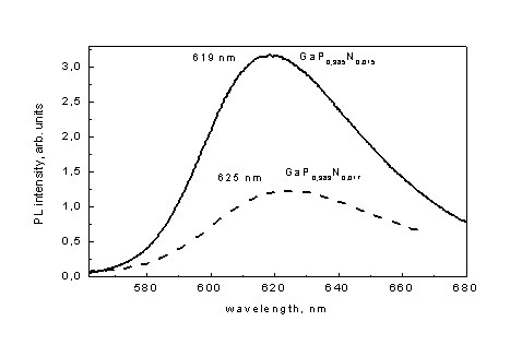 Figure 1.RT PL spectra of GaP1-xNx/GaP, grown at 470 0C (dashed) and 510 0C (solid).
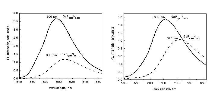
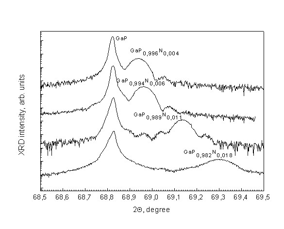
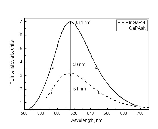 Figure 4. RT PL spectra of GaPAsN/GaP (solid) and InGaPN/GaP (dashed) quantum wells.