| Search for content and authors |
Molecular Beam Epitaxial Growth of GaSb Quantum Dots on Ge Substrates |
| Suwit Kiravittaya 1, Maetee Kunrugsa 2, Suwat Sopitpan 3, Somchai Ratanathammaphan 2, Somsak Panyakeow 2 |
|
1. Naresuan University, Phitsanulok 65000, Thailand |
| Abstract |
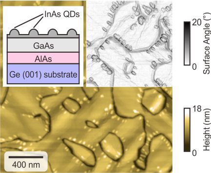
Ge is a well-known bulk material for infrared detectors. Ge doped with transition metals such as gold and mercury have been used for far infrared applications and detectors for CO2 lasers [1]. However, due to its low band gap, typical Ge detectors operate at low temperature of liquid nitrogen. GaSb/GaAs quantum dots (QDs) are type II nanostructures having also a potential for mid-infrared and far-infrared applications [1,2]. Based on quantum confinement behavior, GaSb can operate to operate at higher temperature. We combine these two materials, i.e., Ge and GaSb in our samples grown by molecular beam epitaxy (MBE). At the beginning phase, we grew GaAs epitaxial layer on Ge substrates. Anti-phase domains (APD) of GaAs are distributed on the Ge surface due to the nature III-V compound growth on group IV semiconductors. We have experimentally investigated the growth of GaAs APD on Ge substrates as well as the growth of InAs QDs on APD epitaxial layers [3]. Figure 1 shows an AFM image of InAs/GaAs QDs on Ge substrate. The InAs QDs mainly locate near the domain walls due the high strain field and are elongated along [110] crystallographic directions in each GaAs domain. The elongation directions of APDs are typically perpendicular to each other. For Sb-related growth, we have installed Sb cracker cell to our MBE system and have investigated the growth of GaSb QDs. Figure 2 shows an atomic force microscopy image of typical GaSb QDs having ~7 nm in height and ~80 nm in diameter. Optical properties of these nanostructures are characterized by photoluminescence measurement in order to investigate their quantum confinement behaviors. In this contribution, we will report the MBE growth recipe and characterization of GaSb/GaAs QDs on Ge substrates. Details of our growth steps as well as the properties of obtained structures will be presented. Structural comparisons between conventional QD growth and the growth on Ge substrate will be discussed.
Fig. 1 An AFM image of InAs QDs on APD of GaAs on Ge substrate
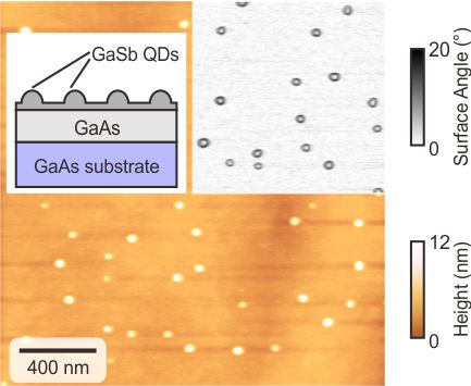
Fig. 2 A typical 2×2 μm2 AFM image of GaSb QDs on GaAs substrate References [1] E H. Putley, "Far infra-red photoconductivity," phys. stat. sol. 6, 571 (1964). K. Kikuchi, M. Saguchi, and A. Oshimoto, "A new photoconductive sensor for 10.6-mm infrared radiation," IEEE Trans. Instrum. Meas. 37, 137 (1988). [2] W.-H. Lin, C.-C. Tseng, K.-P. Chao, S.-C. Mai, S.-Y. Kung, S.-Y. Wu, S.-Y. Lin, and M.-C. Wu, "High-temperature operation GaSb/GaAs quantum-dot infrared photodetectors," IEEE Photon. Technol. Lett. 23, 106 (2011). [3] W. Tantiweerasophon, S. Thainoi, P. Changmuang, S. Kanjanachuchai, S. Rattanathammaphan, and S. Panyakeow, "Self-assembled InAs quantum dots on anti-phase domains of GaAs on Ge substrates," J. Cryst. Growth 323, 254 (2011). |
| Legal notice |
|
| Related papers |
Presentation: Oral at 17th International Conference on Crystal Growth and Epitaxy - ICCGE-17, General Session 8, by Somsak PanyakeowSee On-line Journal of 17th International Conference on Crystal Growth and Epitaxy - ICCGE-17 Submitted: 2013-04-15 08:36 Revised: 2013-05-28 09:30 |