| Search for content and authors |
Field-Emission of Large Scale and Uniform Monolayer Graphene Sheet Supported on Patterned ZnO Nanowire Arrays |
| Lijing Zhang 1, Xiaomiao Liu 2, Qingfeng Yan 1, Xiaoqing Wang 1, Guangqiu Shen 1, Dezhong Shen 1 |
|
1. Tsinghua University, Tsinghua Garden, Beijing 100084, China |
| Abstract |
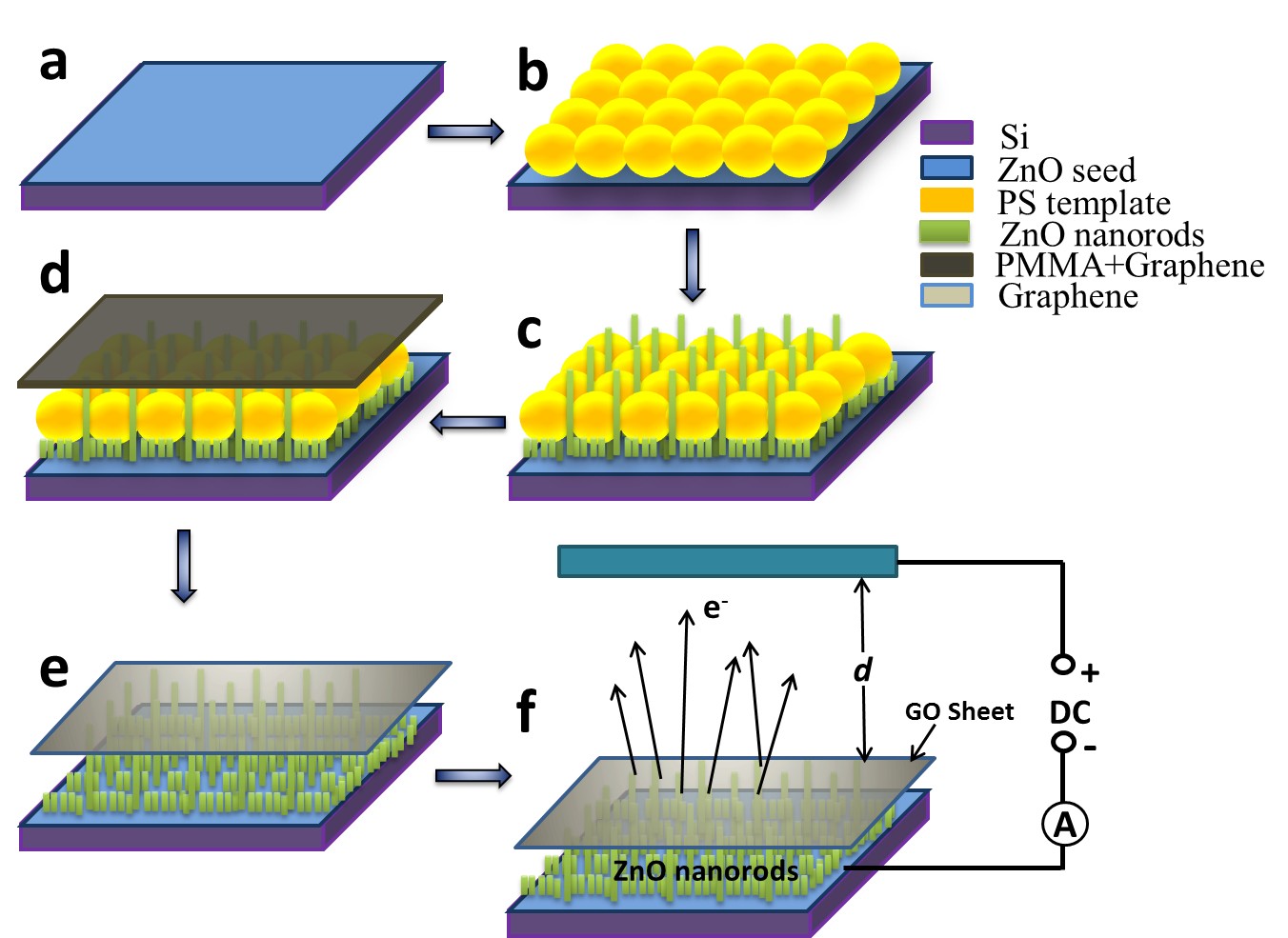
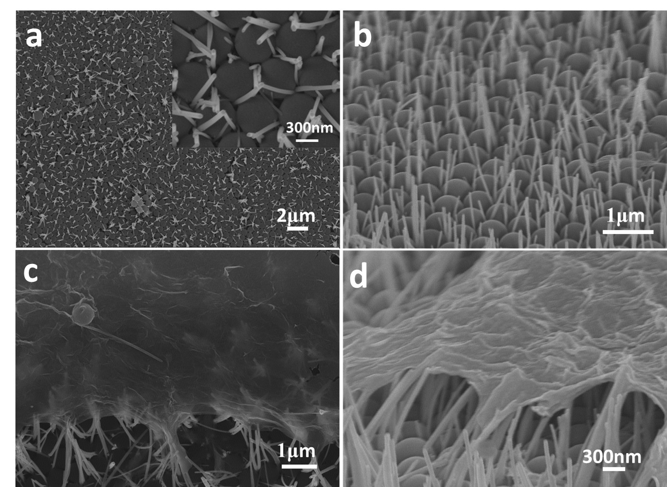
Field emitters possessing needlelike shapes with sharp tips can dramatically reduce the strength of turn-on electric field by several orders of magnitude due to their enhanced local field at these tips. Graphene and its derivatives are expected to be potential field emitters due to their unique electronic properties. The sharp edges of graphene can produce significant enhancement of electron field emission due to the reduction of work function at the edges. Many efforts have been made in exposing the atomically thin edges and fabricating vertical sheets in line with field direction such as screen printing graphene films, photolithographically patterned graphene arrays and graphene sheets supported on metal nanotips. Among them, supporting graphene sheet by well-aligned nanowire arrays can form nanometer-scale sharp protrusions. These high density protrusions localize and enhance the electric field, thereby allowing electrons to tunnel through the tips at very low electric fields and to produce stable emission in a large area. Herein, we demonstrate a facile and effective route toward large scale and uniform graphene sheet supported on patterned ZnO nanowires with nanometer-scale sharp protrusions. The fabrication process is schematically illustrated in Figure 1. Monolayer colloidal crystal template was introduced to tailor the vertical ZnO nanowire (NW). Large-scale colloidal monolayer was prepared by the self-assembly of polystyrene (PS) nanospheres at the air/water interface. It was then transferred on a silicon substrate coated with ZnO seeds. The ZnO nanorods were grown via a hydrothermal growth approach with the colloidal sphere monolayer as a template. The size and period of the ZnO nanowires array synthesized could be controlled by the interstice size and sphere diameter of the colloidal monolayer template. Graphene was originally grown on copper foil by chemical vapor deposition method. The as-grown large area graphene was then transferred onto the patterned ZnO nanowires as a whole sheet by using the polymethyl methacrylate (PMMA) as an interfacial layer. The PMMA-supported graphene/ZnO wires nanocomposites were then washed with acetone followed by annealing in air at 350 °C for 30 minutes to remove the PMMA and PS spheres template as well as to optimize the ZnO nanowires performance. Highly efficient and stable field emission with a low turn-on field was observed from the resulted graphene sheet supported on patterned ZnO nanowire arrays. The enhanced field emission performances were attributed to the patterned and nanometer-scale sharp protrusions which locally enhanced the electric field and dramatically increased the field emission. Fig. 1. A schematic illustration of the fabrication of the graphene/ patterned ZnO nanowires composite. (a) A ZnO seed layer was coated on a silicon substrate, (b) A PS colloidal spheres monolayer was transferred onto the Si substrate, (c) Vertically aligned and patterned ZnO nanowire arrays were synthesized by the hydrothermal growth, (d) Graphene/PMMA film was transferred onto the ZnO nanowire arrays, (e) PMMA and PS template were removed to expose the graphene sheet that uniformly covered the patterned ZnO nanowire arrays, and (f) A schematic of the setup for field emission measurement. Fig. 2. (a) Top-view SEM image of the patterned ZnO nanowires array on a silicon substrate in a large scale. The insert is the corresponding high magnification image. (b) Cross-sectional SEM image of the patterned ZnO nanowires array on the silicon substrate. (c) Top-view and (d) cross-sectional SEM images of the graphene sheets supported by the patterned ZnO nanowires array. Reference [1] Z.C.Yang, Q. Zhao, Y. X. Ou, W. Wang, H. Li, D. P. Yu. Enhanced field emission from large scale uniform monolayer graphene supported by well-aligned ZnO nanowire arrays, Appl. Phys. Lett., 101(2012) 173107. [2] D.X.Ye, S. Moussa, J.D. Ferguson, A. A. Baski, M. S. El-Shall, Highly Efficient Electron Field Emission from Graphene Oxide Sheets Supported by Nickel Nanotip Arrays, Nano Lett., 12 (2012) 1265-1268. [3] C. K. Huang, Y. X. Ou, Y. Q. Bie, Q. Zhao, and D. P. Yu, Well-aligned graphene arrays for field emission displays, Appl. Phys. Lett., 98 (2011) 263104. [4] H. B. Zeng, X. J. Xu, Y. Bando,U. K. Gautam, T. Y. Zhai,X. S. Fang, Fang, B. D. Liu, D. Golberg, Template Deformation-Tailored ZnO Nanorod/Nanowire Arrays: Full Growth Control andOptimization of Field-Emission, Adv.Funct.Mater,19(2009) 3165-3172. |
| Legal notice |
|
| Related papers |
Presentation: Oral at 17th International Conference on Crystal Growth and Epitaxy - ICCGE-17, General Session 8, by Lijing ZhangSee On-line Journal of 17th International Conference on Crystal Growth and Epitaxy - ICCGE-17 Submitted: 2013-04-14 17:16 Revised: 2013-07-17 12:31 |