| Search for content and authors |
Continuous in situ X-ray reflectivity measurement on InGaN epitaxial growth by MOVPE |
| Guangxu Ju 1, Yoshio Honda 1, Masao Tabuchi 2, Yoshikazu Takeda 3,4, Hiroshi Amano 1,5 |
|
1. Garaduate School of Enginnering, Nagoya University (NAGOYAU), Nagoya university, Furo-cyo, Chikusa-ku, Nagoya, Japan, Nagoya 464-8603, Japan |
| Abstract |
High quality InGaN-based quantum wells (QWs) have undergone remarkable development because of their practicalapplications in high-frequency and high-power field-effect transistors, light-emitting diodes, and laser diodes. Metalorganic vapor phase epitaxy (MOVPE) has been the leading technique for the commercial growth of wide band-gap InGaN due to its big market. However, many problems are still unsolved and little is known what is going on during the growth process. Then, in situ measurements for InGaN growth are required to understand the growth of the layers under the growth conditions, and this may help to develop and fabricate better quality InGaN QWs. We have set up an MOVPE chamber installed in alaboratory level X-ray diffractometer (Rigaku RINT-TTRIII). In our previous work, the preliminary experiments of X-ray diffraction (XRD), X-ray crystal truncation rod (CTR) scattering and X-ray reflectivity (XRR) measurements at various growth temperatures of InxGa1-xN growth were reported [1,2]. A combination of these techniques was used for investigation on the In0.09Ga0.91N SQW structures with InGaN of several monolayers (MLs) thickness at 830 °C [3]. Annealed InGaN epilayers and GaN decomposition were also studied by using in situ XRR [4]. However, the measurement time of CTR and XRR measurements is too long to realize real time investigation during the formation of heterostructures, because of measuring with the angle scan. In this work, a continuousin situ XRR observation on InGaN epitaxially grown on free-standing GaN substrate and GaN(2 mm)/sapphire template without the angle scan is reported. The analysis of the strain relaxation of InxGa1-xN epilayers is conducted.
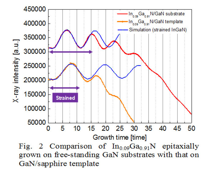
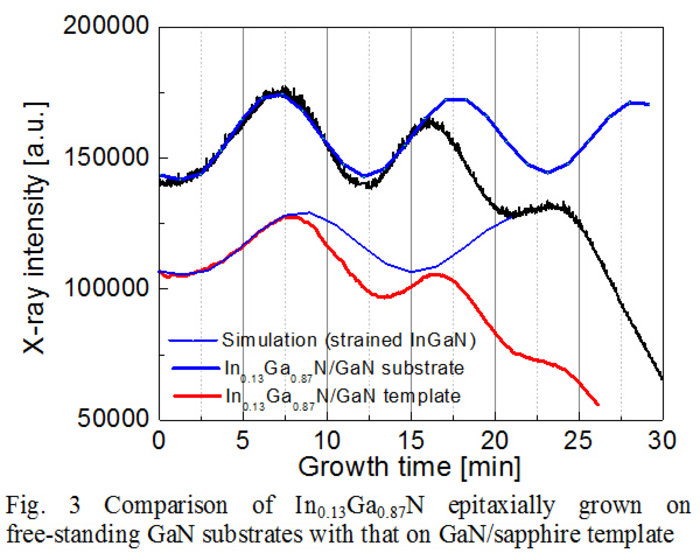
Both the incident and reflected angle of X-rays were fixed at 0.6○. The growth of InxGa1-xN and its continuous XRR measurements were simultaneously started and stopped without interruption. The indium composition was 0.09 and 0.13. In Fig.1, experimentally observed oscillations of XRR (red and black line) with growth time are shown. The red line is for thick In0.09Ga0.91N epilayer and the black one is for thick In0.13Ga0.91N epilayer. Both of them were grown on free-standing GaN substrates. An ideal reflectivity oscillation, assuming fully strained InGaN on GaN, with changing InGaN thickness is shown by the blue line. For the ideal reflectivity oscillation, one period of oscillation corresponds to the InGaN thickness of 8.9 nm. The changing InGaN thickness is equal to the growth time multiplied by the growth rate of InGaN epilayer, and then, the growth rate of InGaN epilayer can be estimated. Decrease of the experimental X-ray intensity with growth time is considered due to the increasing surface roughness of InGaN epilayer caused by the relaxation. It is understood that InGaN is fully strained below the thickness of 14.0 and 8.5 nm with indium composition 0.09 and 0.13, respectively. It is in good agreement with the reported results by D. Holec et al. by calculation using the isotropic approximation and energy balance model [5]. Continuous in situ X-ray reflectivity was also conducted on InGaN epitaxially grown on GaN/sapphiretemplate with indium composition0.09 and 0.13. Figs. 2 and 3 show the comparison of InGaN epitaxially grown on free-standing GaN substrates with that on GaN/sapphiretemplates at each indium composition. These results show that the critical thickness of In0.09Ga0.91N are 14.0 and 8.1 nm and that of In0.13Ga0.87N are 8.5 and 5.3 nm, on free-standing GaN substrate and GaN/sapphire template, respectively. The dislocation density for free-standing GaN substrate and GaN/sapphire template is 2×107 cm-2 and 2.6×109 cm-2 respectively. High dislocation density of the templates accelerates the relaxation in InGaN epilayer, due to thread dislocation extended into the grown layer.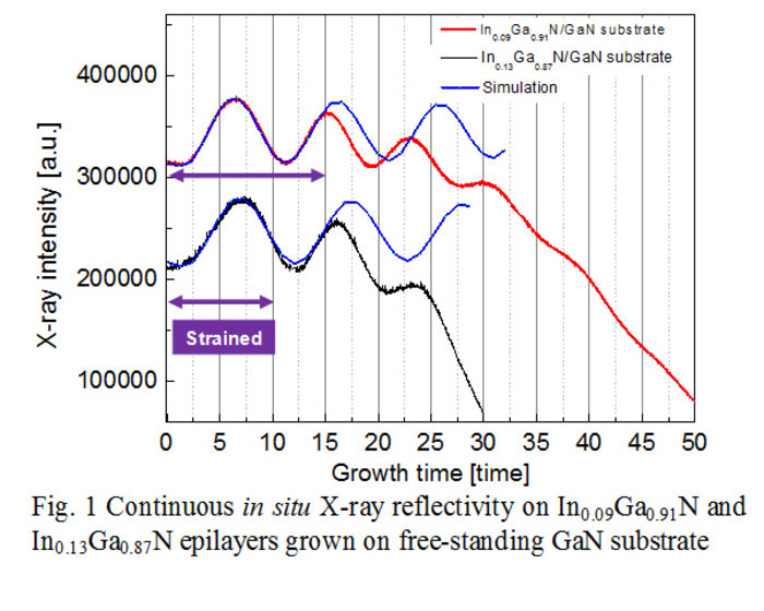
Continuous in situ X-ray reflectivity observation on InGaN epitaxial growth without the angle scan was successfully achieved. The strain relaxation of In0.09Ga0.91N and In0.13Ga0.87N epilayers grown on free-standing GaN substrate was observed. The experimental results agreed with the calculated results using the isotropic approximation and energy balance model. Comparing In0.09Ga0.91N and In0.13Ga0.87N epitaxially grown on free-standing GaN substrates and GaN/sapphire templates, it was clearly and quantitatively observed by XRR that the critical layer thicknesses of InGaN grown on GaN/sapphire templates were thinner than those grown on free-standing GaN substrates.
This work was partly supported by NEDO.
[1] Y. Takeda et al., IOP Conf. Ser.: Mater. Sci. Eng. 24 (2011) 012002. [2] G.X. Ju et. al., J. Cryst. Growth 318 (2011)1143. [3] G. X. Ju et al., J. Cryst. Growth370 (2013) 36. [4] G. X. Ju et al., Jpn. J. Appl. Phys. (in press). [5] D. Holec et al., J. Cryst. Growth 303 (2007) 314. |
| Legal notice |
|
| Related papers |
Presentation: Oral at 17th International Conference on Crystal Growth and Epitaxy - ICCGE-17, General Session 6, by Guangxu JuSee On-line Journal of 17th International Conference on Crystal Growth and Epitaxy - ICCGE-17 Submitted: 2013-04-14 14:27 Revised: 2013-07-19 20:16 |