| Search for content and authors |
Application of microwave spectroscopy to studies of electron transport properties |
| Agnieszka Wołoś 1,2, Aneta Drabińska 2 |
|
1. Polish Academy of Sciences, Institute of Physics, Lotnikow 32/46, Warsaw 02-668, Poland |
| Abstract |
| Many research laboratories in the world are equipped with EPR (Electron Paramagnetic Resonance) spectrometers dedicated to investigations of paramagnetic defects in crystalline materials. Whereas conducting samples placed in a microwave cavity of the spectrometer can show also features related to their magnetoconductivity. A condition necessary to observe these types of signals is presence of electric component of microwave field in the spot where the investigated sample is placed. This may require the use of specially designed resonators, such as these exploiting TM010 mode. It turns out, however, that in a popular TE102 rectangular cavity dedicated to investigations of magnetic dipole transitions, and thus such requiring absorption of a quantum of microwave magnetic field, the electric field component of microwaves spontaneously occurs in the center of the cavity due to disruption of the perfect distribution of microwave field by the presence of the sample and quartz elements of the cryostat. In such a resonator, we observe signals related to magnetoconductivity which may constitute an undesired background or an interesting object for study. We will shortly introduce such features recorded for different novel materials, GaN/AlxGa1-xN heterostructures, graphene, and topological insulators.
At the GaN/AlxGa1-xN interface, the two-dimensional electron gas forms spontaneously with typical sheet electron concentration of the order of 1012 – 1013 cm-2. The frequency of the popular microwave X-band is close but slightly higher than the typical plasma frequency in mm-sized GaN/AlxGa1-xN samples, allowing thus to observe edge magnetoplasma resonance in the X-band EPR spectrometer [1,2], Fig. 1(a). It has been recently reported, that similar conditions are as well fulfilled for the two-dimensional electron system in MgxZn1-xO/ZnO [3]. The magnetoplasma resonance, the coupled plasmon-cyclotron resonance, allows to determine electron concentration and mobility without having to make electric contacts. It allows to probe electric parameters even when the substrate is conductive or the structure contains conducting interfaces. The effective masses can be also investigated in this way [3]. Additionally, Shubnikov – de Haas oscillations can be also observed in EPR spectrometers, if only the applied magnetic field is high enough [1, 4, 5], Fig. 1(b). In general, the observation of both cyclotron or plasmon-cyclotron resonance and Shubnikov – de Haas oscillations requires high-mobility samples, as both the line width of the resonance line and the magnetic field onset for Shubnikov – de Haas signal scale with the mobility. Low-field magnetoconductivity related to quantum effects of weak localization and antilocalization can be as well successfully investigated with the use of the EPR spectrometer. Modern spectrometers allow to inverse the direction of the magnetic field with very smooth zero crossing. Fig. 1(c) shows examples of weak localization and antilocalization phenomena measured for graphene [6], Bi2Te2Se topological insulator, and GaN/AlxGa1-xN heterostructure. These are non-resonant signals, arising due to changes of the cavity quality factor induced by the change in sample conductivity. Unlike the previous case, one can investigate low-mobility samples, so as many scattering events occur before electron wave function loses its ability to interfere. For such a condition, it is a DC measurement, although microwave frequency is used to probe the sample. Cyclotron resonance due to relativistic Fermions in Bi2Te3 topological insulator is shown in Fig.1(d). In a case of topological insulators from bismuth compound family, high bulk conductivity due to high concentration of native crystal lattice defects is a major obstacle to observe cyclotron resonance of topological surface states using optical transmission method or electric transport. Placing the sample in a resonance cavity provided so far the only way for observation of this phenomenon [5]. We would like to acknowledge teams of A. Hruban and W. Strupinski from the Institute of Electronic Materials Technology, Warsaw, C. Skierbiszewski from the Institute of High Pressure Physics, Unipress, Warsaw, and Z. Zytkiewicz from the Institute of Physics Polish Academy of Sciences, Warsaw for supplying us with samples for the studies. We would like to thank Prof. M. Kaminska for many fruitful discussions. This work was partially supported by the NCN grant no 2011/03/B/ST3/03362, Poland and NCBiR grant GRAF-TECH/NCBR/02/19/2012, Poland.
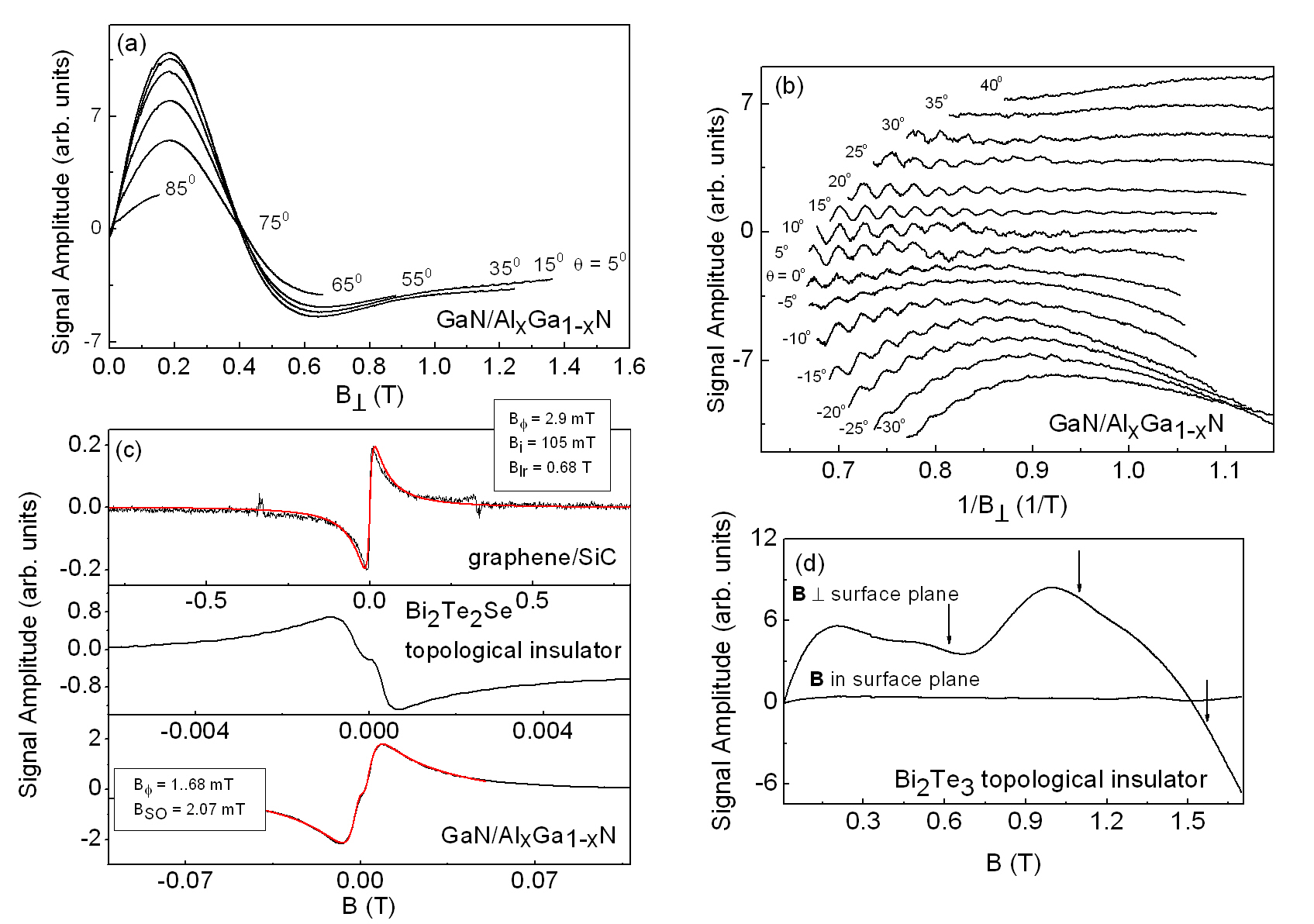
Figure 1. Signals recorded with the use of X-band EPR spectrometer. The temperature is about 5 K. (a) Edge magnetoplasma resonance in GaN/AlxGa1-xN heterostructure. The angle between the direction of the magnetic field and the GaN c-axis (perpendicular to the plane of the two-dimensional electron gas) is given for each spectrum. (b) Shubnikov – de Haas oscillations in GaN/AlxGa1-xN heterostructure dependent on the perpendicular to the sample plane component of the applied magnetic field. (c) weak localization (WL) and antilocalization (WAL) signals in: graphene grown on SiC (WL), Bi2Te2Se topological insulator (WL+WAL), GaN/AlxGa1-xN heterostructure (WL+WAL). Fitted parameters are given. (d) Cyclotron resonance of relativistic Fermions in Bi2Te3 topological insulator. Arrows indicate position of the three distinguished resonance lines. |
| Legal notice |
|
| Related papers |
Presentation: Invited oral at 17th International Conference on Crystal Growth and Epitaxy - ICCGE-17, General Session 5, by Agnieszka WołośSee On-line Journal of 17th International Conference on Crystal Growth and Epitaxy - ICCGE-17 Submitted: 2013-04-11 14:01 Revised: 2013-04-11 14:16 |