| Search for content and authors |
Comparative Study of Transport Properties in AlInSb/InSb and AlInSb/InAsSb Quantum Wells |
| Takusi Manago 1, Shuichi Ishida 2, Hirotaka Geka 3, Ichiro Shibasaki 4 |
|
1. Fukuoka University, 8-19-1 Nanakuma, Jonan, Fukuoka 814-0180, Japan |
| Abstract |
| Two-dimensional electron systems (2DES) using narrow-gap semiconductors are important for high speed devices, infrared detectors, highly sensitive magnetic sensors and spintronic applications, because of high electron mobility and large effective g-factor. We have studied the well-width dependence of sheet resistivity, carrier density and mobility in Al0.1In0.9Sb/InSb and Al0.1In0.9Sb/InAs0.1Sb0.9 QWs, and found that the transport properties of InSb and Al0.1In0.9Sb QWs are entirely different especially in low temperature. In this paper, we explain the result, based on the calculated band-alignment of these QWs.
The samples were grown by molecular beam epitaxy (MBE). The sample structures are GaAs cap (6.5 nm) /Al0.1In0.9Sb cap (50 nm)/InSb or InAs0.1Sb0.9 active layer (Lw)/Al0.1In0.9Sb buffer (700 nm)/GaAs (100) substrate. The layer structures are the same except the active layer for both QW structures. The substrate is a semi-insulating GaAs and all layers are undoped. The well width (Lw) of the active layer is 15 ~ 200 nm. As shown in Fig.1, the resistivity in low temperature of InAs0.1Sb0.9 QWs is much smaller than that of InSb QWs. The difference has been found to result from the band alignment calculated for these QW structures. Fig.2 indicates that the bottom of the conduction band of InSb QWs is depleted above the Fermi level (EF), while that of InAs0.1Sb0.9 QWs is just under EF in low temperature. In addition, the mobility of InSb QWs falls markedly with decreasing Lw, while that of the InAs0.1Sb0.9 QWs hardly depends on the well width. The mobility decrease with narrowing Lw could originate from the possible strain-effect due to the lattice mismatch. This work was partly supported by the Japan Society for the Promotion of Science (JSPS), Grant-in-Aid for Scientific Research (C: 24560034).
|
| Legal notice |
|
Presentation: Poster at 17th International Conference on Crystal Growth and Epitaxy - ICCGE-17, General Session 8, by Shuichi IshidaSee On-line Journal of 17th International Conference on Crystal Growth and Epitaxy - ICCGE-17 Submitted: 2013-04-11 08:49 Revised: 2013-07-23 15:54 |
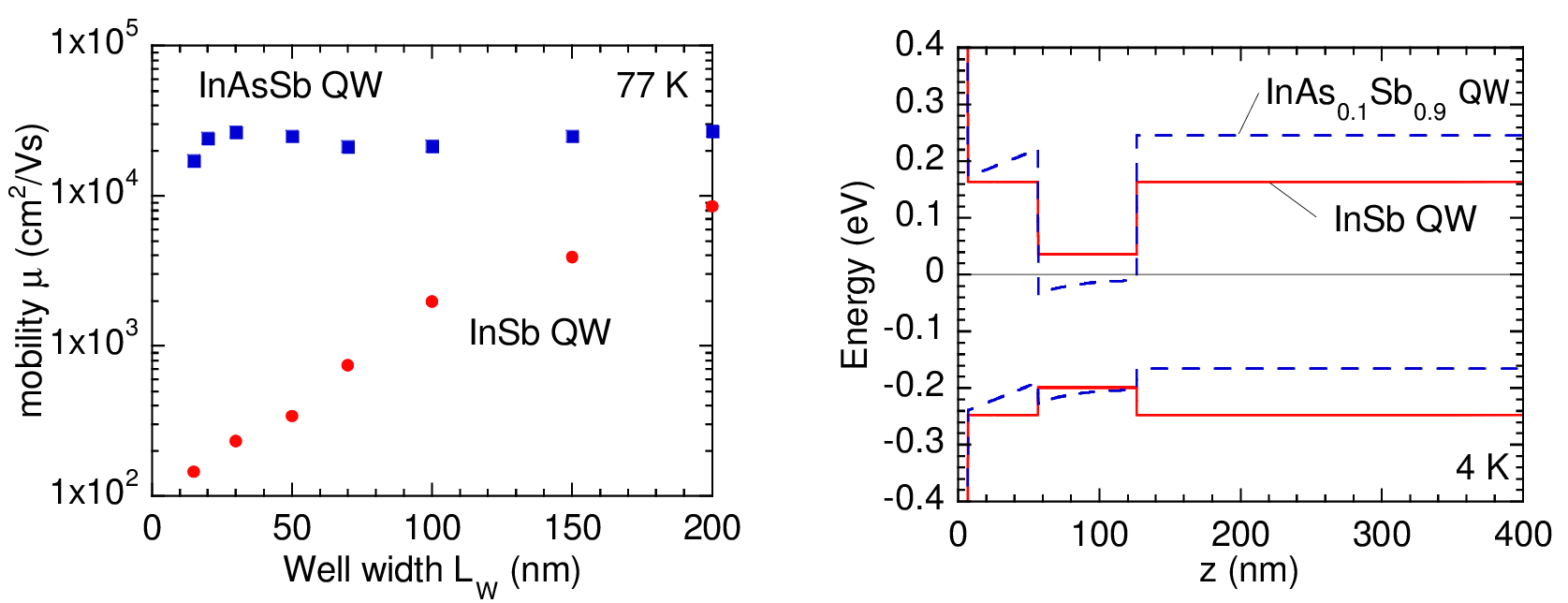 Fig.1 Well-width dependence of mobility Fig.2 Energy-band diagram for Lw =70 nm