| Search for content and authors |
An Investigation on Optical and Structural Properties of Nanocrystalline CdTe Thin Films Growth by Employing a New Vapor Flow Controlling System |
| Fatemeh Hosseini Siyanaki , Shiva Khorramabadi , Hamid Rezagholipour Dizaji 1, Mohammad H. Ehsani |
|
1. Semnan University, Physics Department, Crystal Growth Lab., Tehran 35195-363, Iran |
| Abstract |
Cadmium Telluride (CdTe) polycrystalline layers can be prepared by several techniques among which, vacuum thermal evaporation is known as a suitable one to produce nanocrystalline thin films [1]. CdTe is regarded as one of the most promising absorber material for fabrication of high efficiency thin film solar cells [2]. In the present investigation, Cadmium CdTe thin films with thickness of 350nm, and grain sizes between 15nm to 40nm have been prepared by vacuum thermal evaporation technique, conventional and the one in which a novel vapor flow controlling system was employed. This system, as shown in Fig.1, consists of a rotating cylinder with one semi-closed end named shutter. The shutter includes two slits and is in the vicinity of the substrate. The other end of cylinder is completely open and close to the source. Placing this equipment in the way of vapor flux from the source to the substrate cut the depositing flux of vapor periodically and can change the way of vapor flux. It led to considerable change of optical properties, nanocrystalline structure, and also stochiometery of the thin films. 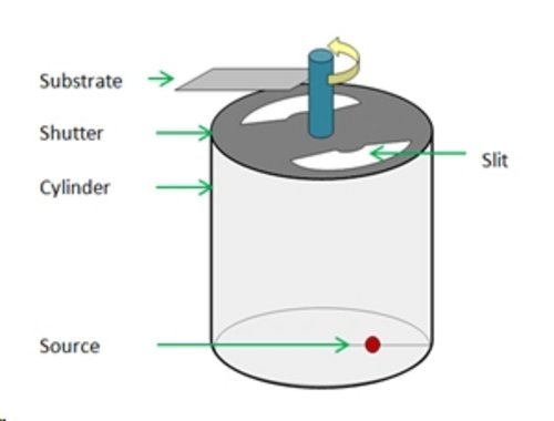 Figure 1: Schematic view of the vapor flow controlling system The thin film deposited by conventional thermal evaporation method named S1, and the ones prepared by using the shutter and cylinder at 25, 50 and 75 rpm rate of rotation named S2, S3 and S4 respectively. Three other samples were prepared by applying the shutter alone, i.e. without the cylinder. They deposited at 25, 50 and 75 rpm rate of rotation and named S5, S6 and S7 respectively. The optical parameters such as absorption coefficient, bandgap, refractive index, and structural parameters such as texture coefficient, preferential orientation factor, crystallite size, were obtained. Also EDAX and FESEM result of samples were compared with each other in this study. The most considerable increase in absorption coefficient was observed in S7 (9.8×104 cm-1) in comparison with S1 (5.5 ×104 cm-1 ) at 520nm wavelength of light (Fig. 2). By increasing the absorption coefficient, the light can be absorbed in a thinner layer of substance, considering following formula:I/I0= exp (αd) (1) In this formula α is absorption coefficient and d is a thickness of film in which a light with intensity of I0 reduce to I because of absorption [3]. Therefore it seems that S7 is highly preferable in providing thinner layer of CdTe with similar result in absorbing the light. The most considerable change in the bandgap also was observed in S6 (1.66 eV) in comparison with S1 (1.54 eV). The changes of XRD patterns of S6 and S7 in comparison with S1 are illustrated in Fig. 3. 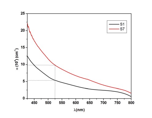
Figure. 2 absorption coefficient of S1 and S7 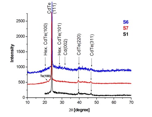 Figure. 3 XRD pattern of S1, S6, and S7. The reasons and consequences of mentioned changes investigated by analyzing the structural and optical parameters of films, and will be presented in details. References [1] S. J. Ikhmayies and R. N. Ahmad-Bitar, “Optical Properties of Nanocrystalline CdTe Thin Films”, Phys. B., 405 (2010) 3141. [2] V. D. Novruzov, et. al., “CdTe thin film solar cells prepared by a low-temperature deposition method”, Phys. Status Solidi A 207 (2010) 730. [3] M. Ohring, “The Materials Science of Thin Films’, Academic Press, 1992. |
| Legal notice |
|
| Related papers |
Presentation: Poster at 17th International Conference on Crystal Growth and Epitaxy - ICCGE-17, General Session 10, by Hamid Rezagholipour DizajiSee On-line Journal of 17th International Conference on Crystal Growth and Epitaxy - ICCGE-17 Submitted: 2013-04-07 20:15 Revised: 2013-07-25 11:57 |