| Search for content and authors |
The Determination of Different Types of Conductivity Areas within Homogeneity Region of Ga Solid Solutions in PbTe films on Si-substrates |
| Alexander M. Samoylov 1, Sergey V. Belenko 1, Pavel V. Seredin 1, Staislav V. Ryabtsev 1, Alexandr E. Klimov 2 |
|
1. Voronezh State University (VGU), Universitetskaya Sq., 1, Voronezh 394006, Russian Federation |
| Abstract |
| The thin films and single crystals of Ga-doped PbTe are the perspective materials for detecting the infrared (IR) irradiation in the middle wave range [1]. The IR sensitivity of these materials is similar to that of Cd1–xHg
x
Te but processing procedures are much less demanding. Under the influence of the presence of III A group metals the energy spectrum of PbTe and its solid solutions can change significantly and depends on not only the concentration of impurity atoms but from the method of synthesizing of the investigated samples [2].
The main purpose of this work is to determine the borders of areas with different types of conductivity within homogeneity region of Ga solid solutions in PbTe/Si and PbTe/SiO2/Si films prepared by modified HWE technique. The chemical composition of Ga-doped PbTe/Si and PbTe/SiO2/Si layers was analyzed by the electron probe microanalysis (EPMA) method on JEOL JCA 840 with the help of the energy dispersion (ED) and the wave dispersion (ED) spectrometers using Kα1 - and Lα1 - emissions. The electrical parameters of PbTe<Ga> films were evaluated from dc four-probe measurements by Van der Pauw technique and by the investigation of the C - U - curves ("Hg probe" method) also. As it is known, the oxidation process of AIVBVI semiconductors, which intentionally or unintentionally occurs on the surface, affects the electronic properties of these materials greatly. In order to reduce this undesirable influence the silver contact pads were prepared by the thermal deposition in vacuum immediately after the plasma etching of PbTe<Ga>/Si and PbTe<Ga>/SiO2/Si heterostructures surface through a special mask in Ar atmosphere within the same technological cycle. 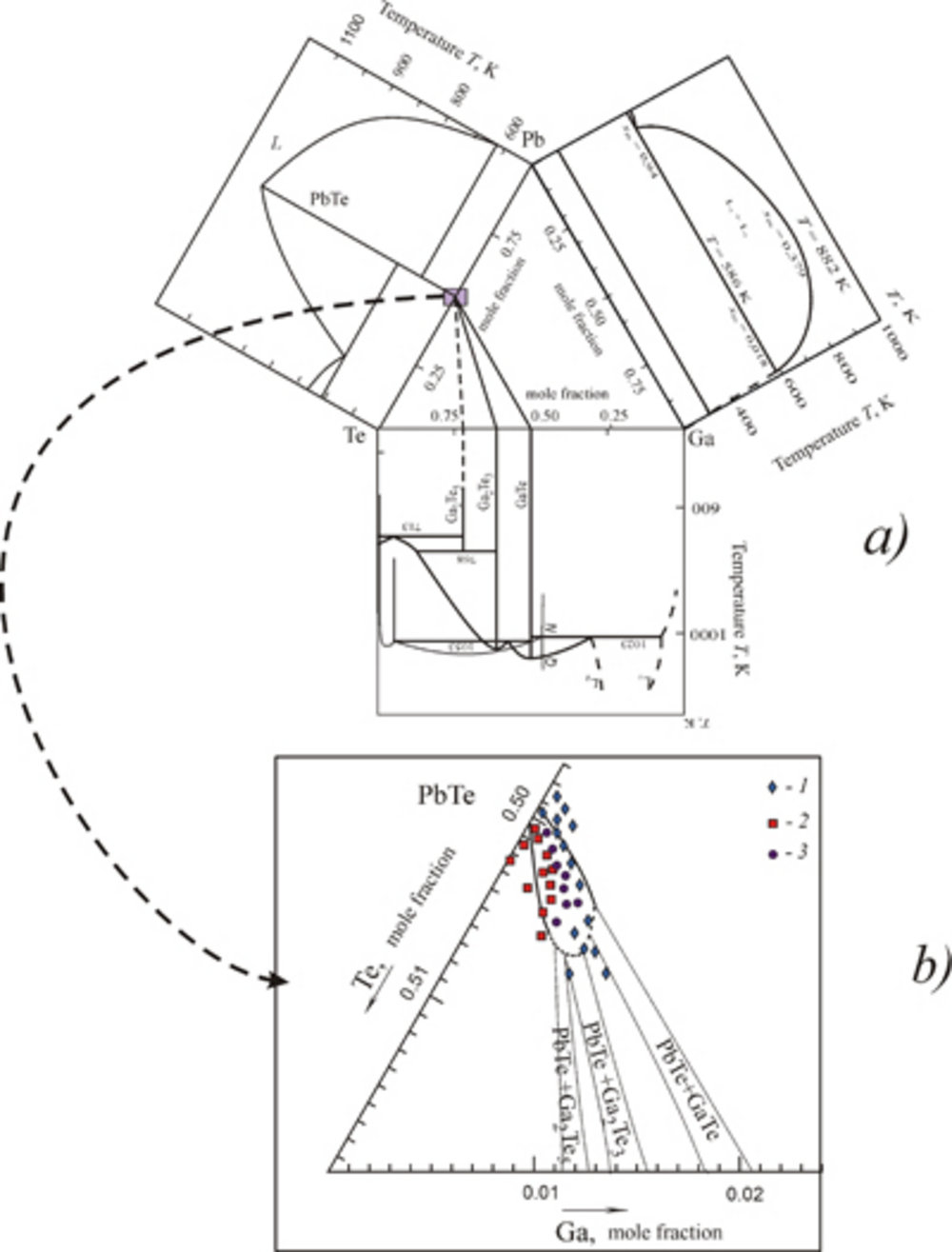 Fig. 1. The region of Ga solubility in PbTe/Si (100) and PbTe/SiO2/Si (100) films from the point of view of the ternary Ga - Pb - Te system (a), and the areas with different types of conductivity within homogeneity region of Ga solid solutions (b); 1 - samples with n-type of conductivity, 2 - samples with p-type of conductivity, 3 - samples with semi-insolating properties. For measurements of the electrical parameters of PbTe/Si and PbTe/SiO2/Si heterostructures two series of samples have been prepared. The first doping procedure is based on a two-zone annealing of previously formed undoped PbTe/Si and PbTe/SiO2/Si films in the saturated vapor which corresponds to the three-phase equilibrium L1 - GaTe(S) - V in Ga - Te binary system. lead telluride samples with little excess of Te atoms have been chosen for this two stage doping procedure. These PbTe1+δ films (0.0008 < δ < 0.006) have usually the p-type of conductivity and charge carrier densities of about 1015 -1017 cm–3 at 77 K. Fig. 1. The region of Ga solubility in PbTe/Si (100) and PbTe/SiO2/Si (100) films from the point of view of the ternary Ga - Pb - Te system (a), and the areas with different types of conductivity within homogeneity region of Ga solid solutions (b); 1 - samples with n-type of conductivity, 2 - samples with p-type of conductivity, 3 - samples with semi-insolating properties. For measurements of the electrical parameters of PbTe/Si and PbTe/SiO2/Si heterostructures two series of samples have been prepared. The first doping procedure is based on a two-zone annealing of previously formed undoped PbTe/Si and PbTe/SiO2/Si films in the saturated vapor which corresponds to the three-phase equilibrium L1 - GaTe(S) - V in Ga - Te binary system. lead telluride samples with little excess of Te atoms have been chosen for this two stage doping procedure. These PbTe1+δ films (0.0008 < δ < 0.006) have usually the p-type of conductivity and charge carrier densities of about 1015 -1017 cm–3 at 77 K.
The second method of PbTe<Ga>/Si and PbTe<Ga>SiO2/Si heterostructures preparation offers the direct one stage synthesis, in which the doping and the layer condensation processes proceed simultaneously [3]. The results of high-temperature mass-spectroscopy study have shown that at temperature interval 950 - 1300 K the saturated vapor phase over Ga1–xPb x melts is enriched by III A group metal regarding to the Raoult's law [4]. Varying the ratio of partial pressures of the metal components and the chalcogen, it is possible to synthesize Pb1–zGa z Te layers (0.0011 < z < 0.08), in which the tellurium content has been varied within the limits from 0.485 up to 0.525 mole fraction. X-ray, SEM, and EPMA experimental data have demonstrated that the region of homogeneous Pb1–zGa z Te films existence was much narrow than indicated interval of Ga concentration in prepared samples [3]. It has been noted that homogeneity region of Ga - solid solutions in PbTe/Si and PbTe/SiO2/Si is asymmetric regarding to quasibinary PbTe - GaTe cross-section (Fig. 1 a) The comparison of the electrical parameters results measurements with the region of homogeneous Ga solid solutions in PbTe films existence is presented in Fig. 1 b. It can be seen that the areas with n- and p-types of conductivity exist within homogeneity region of Ga solid solutions in PbTe/Si and PbTe/SiO2/Si films [5]. Besides, the samples with semi-insolating properties ([n], [p] are about 1013 - 1014 cm–3 at T = 77 K), which are perspective for fabrication of IR sensors, have been observed. It has been found that the area of existence of PbTe<Ga> films with the semi-insolated properties has the complicated shape. Along PbTe - GaTe and PbTe - Ga2Te3 cross-sections the maximum concentration of Ga atoms zGa is approximately 0.0076 ± 0.0005. References 1. M. Rahim, A. Khiar, M. Fill, F. Felder, H. Zogg. Electron Lett. 18, 1037 (2011). 2. B.A. Volkov, L.I. Ryabova, D.R. Khohlov. Progress in Phys. Sci. (Russ). 172, 875 (2002). 3. S.V. Belenko [et al]. Journ. Surface Investig. X-ray, Synchrotron and Neutron Techn. 4, 170 (2010). 4. A.M. Samoylov [et al]. Russian Journ. General Chem. 81, 27 (2011). 5. A.M. Samoylov, S.V. Belenko, M.K. Sharov, E.A. Dolgopolova, V.P. Zlomanov. Journ. Cryst. Growth. 351, 149 (2012). |
| Legal notice |
|
| Related papers |
Presentation: Poster at 17th International Conference on Crystal Growth and Epitaxy - ICCGE-17, Topical Session 4, by Alexander M. SamoylovSee On-line Journal of 17th International Conference on Crystal Growth and Epitaxy - ICCGE-17 Submitted: 2013-04-06 08:05 Revised: 2013-07-23 17:58 |