| Search for content and authors |
Crystal growth of novel single crystals for electro-optical applications |
| Kiyoshi Shimamura 1,2, Encarnacion Garcia Villora 1 |
|
1. National Institute for Materials Science (NIMS), Tsukuba 305-0044, Japan |
| Abstract |
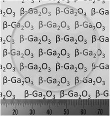
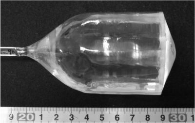
Recently, optical technology progress in a wide range of applications, and still demands the further development. Since conventional crystal materials face some of the limitations, these issues require new optical single crystals. Here, novel single crystals, which have advantageous characteristics toward the above demands, will be introduced. β-Ga2O3 exhibits the largest band gap (Eg = 4.8 eV) among the transparent conductive oxides (TCOs). 1 and 2 inch size β-Ga2O3 single crystals were grown by the FZ and EFG techniques, respectively. Epitaxial growth of c-plane wurtzite InGaN-MQW on a-plane β-Ga2O3 was realized by the MOCVD technique. Vertical structured blue LEDs on β-Ga2O3 with different packaging styles were demonstrated. Tb3(Sc1-xLux)2Al3O12 (TSLAG) single crystals with 1 inch in diameter have been designed and grown for high-power laser machinery. TSLAG showed a higher visible transparency and a larger Faraday rotation than Tb3Ga5O12. TSLAG is therefore very promising material in particular for new magneto-optical isolator applications in the VIS-NIR wavelength. High-brightness LEDs (HB-LEDs) are facing several difficulties such as temperature- and photo-degradation of Ce:YAG powder phosphor and epoxy dome containing them. A new concept of white LEDs based on Ce,Gd:YAG single crystal phosphor plates (SCPPs), which are able to overcome the above issues, is proposed. SCPPs demonstrated excellent thermal stability with no temperature quenching, high values of luminous efficacy and increased quantum efficiency. Acknowledgements: Authors would like to thanks to Mr. K. Aoki of Koha Co., Ltd., Dr. D. Inomata of Tamura Corp., and Mr. T. Hatanaka, Mr. A. Funaki, Mr. T. Kizaki and Mr. K. Naoe of Fujikura Ltd., for the collaboration.
Fig.: 2-inch size β-Ga2O3 single crystal wafer grown by the EFG technique (left) and magneto-optical Tb3(Sc1-xLux)2Al3O12 single crystal grown by the Czochralski technique (right). |
| Legal notice |
|
Presentation: Invited oral at 17th International Conference on Crystal Growth and Epitaxy - ICCGE-17, Topical Session 6, by Kiyoshi ShimamuraSee On-line Journal of 17th International Conference on Crystal Growth and Epitaxy - ICCGE-17 Submitted: 2013-04-01 00:56 Revised: 2013-04-01 01:27 |