| Search for content and authors |
Imaging defects during growth of seeded directionally solidified mono-like silicon for photovoltaic applications |
| Maria Tsoutsouva 1, Denis Camel 2, Thu Nhi Tran Thi 1, José Baruchel 1, Benoit Marie 2, Vanessa Amaral de Oliveira 2, Tamzin Lafford 1 |
|
1. European Synchrotron Radiation Facility (ESRF), Grenoble 38043, France |
| Abstract |
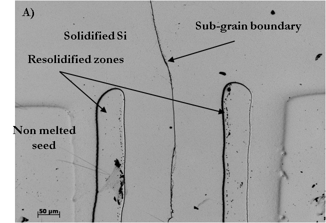
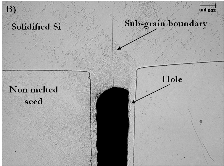
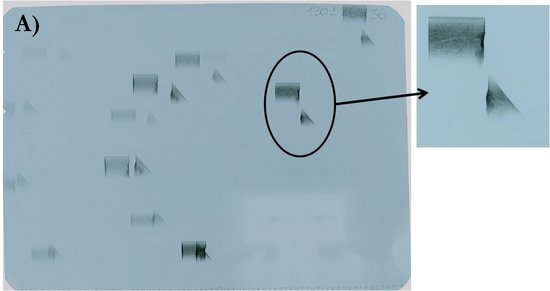
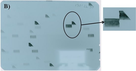
The main challenge of industrial-scale production of photovoltaic devices is the growth of large, high quality Si monocrystals at a much lower cost than that of microelectronics quality crystals. Directional solidification has become a very promising method for achieving this. With the use of an extended monocrystalline seed, high quality “mono-like” Si crystals [1, 2] can be grown. However, multiple seeds are needed in order to grow large crystals and that fact raises the question of growth at the boundary between seeds. In the present work, we investigate the early stages of Si solidification in the region where the liquid Si penetrates between two seeds, and the evolution of the crystal growth from this region. Synchrotron radiation Bragg imaging (white beam, monochromatic section topography, “weak beam” images) was applied to samples grown from melted silicon on oriented seeds with a small gap between them. The images showed the subgrain boundary and even very low subgrain misorientation could be measured, while the generation and evolution of dislocations during growth was followed. Besides X-ray diffraction imaging, Scanning Electron Microscopy (SEM) and micro-Fourier Transform Infrared Spectroscopy (μ-FTIR) mapping were applied, the latter showing the elemental distributions of oxygen, iron and carbon. In the present study, two cases are examined of samples cut parallel to the growth directionas shown in the SEM images in Figure 1. In Figure 1A we observe the presence of two distinct, vertical, resolidified zones between the seeds; and in Figure 1B, the existence of a hole is observed in the same area. As the regrowth proceeded from the seeds, the presence of a sub-grain boundary was observed between the two seeds in both cases. With the aid of white beam image topography (Figure 2) we observe that in both cases the solidified Si is built of two separate sub-grains which are slightly misoriented but both of them are well crystallized and follow the crystallographic orientation of the seed. However, in case A, networks of dislocations are generated at the top edges of the resolidified zones, while in case B, no such bunches of dislocations are observed.
Figure 1: SEM images of the solidified zone between the seeds, parallel to the growth direction, for the two cases that are studied. Figure 2: White beam diffraction images, of the solidified zone between the seeds, for the two cases, showing the misorientation between the two subgrains. Dislocations are associated with deterioration in the minority carrier lifetime as measured using the Light-Beam Induced Current method. μ-FTIR mapping showed a particular distribution of contaminants in the resolidified zones in case A. A model is proposed in order to explain the probable formation mechanism of the resolidified zones between the seeds during the solidification process, and their possible influence on the observed development of a dislocation network is discussed. [1] A. Jouini et al., Prog. Photovolt: Res. Appl.20 (2012 ) 735-746 [2] M. Trempa et al., J. Cryst. Growth 351 (2012) 131-140 |
| Legal notice |
|
| Related papers |
Presentation: Invited oral at 17th International Conference on Crystal Growth and Epitaxy - ICCGE-17, General Session 7, by Maria TsoutsouvaSee On-line Journal of 17th International Conference on Crystal Growth and Epitaxy - ICCGE-17 Submitted: 2013-03-30 23:08 Revised: 2013-07-19 23:42 |